
The Input Capacitor and the Hot Loop
The one loop on the board that carries a square wave of current.
- Lesson 6 of 10
- Intermediate
On a buck converter there is exactly one loop that carries a square wave of current. Not a smoothed version of one. A real square wave, switching from zero to the full inductor current and back, hundreds of thousands of times a second.
That loop runs from the input capacitor, through the high-side switch, into the inductor, and back to the capacitor through ground. It is called the hot loop, and its physical size does more for or against your board than almost any other layout decision.
Quick answer. As close as physically possible, with the shortest and widest connection the footprint allows. The input capacitor supplies the pulsed current the switch demands, and the loop between them has inductance proportional to its area. That inductance turns the switching edge into voltage spikes on the input rail and makes the loop an efficient radiator. Schematic proximity means nothing; only the copper matters.
Why the current is pulsed
Lesson 1 established the asymmetry. While the high-side switch is closed, current flows from the input into the inductor. While it is open, the input side carries nothing at all.
So the input of a buck converter does not draw a steady current. It draws the full inductor current for a fraction D of each cycle and zero for the rest. The source upstream cannot supply that, because the wiring to it has inductance and cannot change current quickly. Something nearby has to supply the pulses, and that something is the input capacitor.
This is the same reasoning as decoupling a digital device, and it is the same geometry. If you worked through the power integrity course, the lesson on what a decoupling capacitor does is describing this situation with a smaller transient.
How much current it carries
The input capacitor carries the difference between the steady current drawn from the source and the pulsed current drawn by the switch. The RMS value of that difference, for a buck in continuous conduction, is:
I_CIN(RMS) = I_OUT · √(D · (1 − D))
For the running example, 12 V to 3.3 V at 2 A, so D = 0.275:
I_CIN(RMS) = 2 × √(0.275 × 0.725) I_CIN(RMS) = 2 × √0.1994 I_CIN(RMS) = 2 × 0.4465 I_CIN(RMS) = 0.893 A
Nearly 900 mA of RMS current through the input capacitor, to deliver 2 A at the output. That is not a rounding error, and it is why the input capacitor's ripple current rating is a real selection criterion rather than a formality.
The expression peaks at D = 0.5, where it equals half the output current:
I_CIN(RMS) = 2 × √(0.5 × 0.5) = 2 × 0.5 = 1.0 A
So the worst case for input capacitor current is an output at half the input voltage. A 12 V to 5 V converter stresses its input capacitor harder than a 12 V to 3.3 V one at the same load, which is not obvious from the schematic.
Why distance becomes voltage
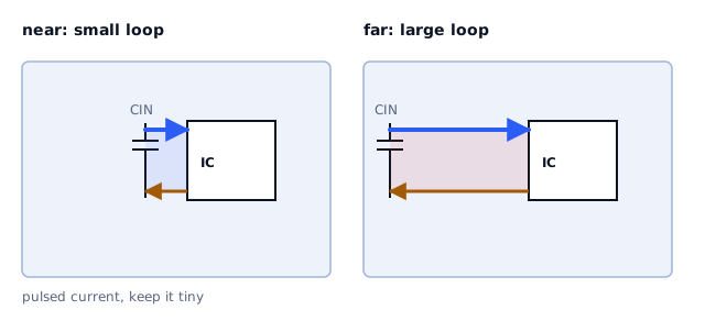
The loop has inductance. Current changing at di/dt through inductance L produces a voltage V = L · di/dt, and both terms here are unfriendly.
The current step is the full inductor current, around 2 A in this example. The transition time is whatever the switch manages, commonly a few nanoseconds in a modern part. Two amps in five nanoseconds is a rate of 4 × 10⁸ A/s.
Through even a small loop inductance, that produces a substantial voltage spike. A loop of a few nanohenries, which is what a few extra millimetres of separation costs you, turns into volts of overshoot on the input pin.
Three consequences follow:
- The switch node rings. Overshoot and ringing stress the switch and can
exceed its absolute maximum rating.
- The loop radiates. A loop carrying a square wave of current with fast
edges is an efficient magnetic antenna, and its effectiveness scales with enclosed area.
- The input rail is polluted. The spike appears on the rail that feeds
everything else on that supply.
The quantity doing the damage is the one the power integrity course calls loop inductance, and it is set by enclosed area here exactly as it is there.
What "close" means in practice
Texas Instruments identifies the input capacitor and power ground loop as the most critical PCB feature of a buck converter, and the guidance in its datasheets is consistent: place input capacitors as close as possible to the device's input and ground pins, with wide and short traces and the smallest loop area achievable.
Concretely, on a modern integrated regulator:
- The smallest ceramic input capacitor goes adjacent to the IC pins,
typically on the same side, with its pads almost touching the device's input and ground pads.
- Its ground connection goes to the device's power ground by the shortest
copper available, not by a via to a plane and back if that makes the loop bigger.
- Larger bulk capacitance goes further out. It is not in the fast loop and
does not need to be, because it is handling lower-frequency variation.
- Vias in the hot loop add inductance. Where the loop must change layer, use
several vias in parallel rather than one.
The order matters: small and close first, bulk second. A 47 µF electrolytic at the board edge plus a 100 nF at the pins is a far better input stage than a 47 µF at the pins and nothing else, because the fast edge needs low inductance rather than capacitance.
The thing that makes this invisible
On the schematic, the input capacitor is next to the IC. It is drawn right there, one net away. Nothing about the schematic distinguishes a layout with a 2 mm loop from one with a 20 mm loop.
This is why input capacitor placement is a layout review item rather than a schematic review item, and why it belongs on the checklist in the grounding course alongside the other return path checks. The return side of this loop is a return path like any other, and the same reasoning about loop area applies to it.
How to check yours
- Find the input capacitor, the high-side switch and the ground return.
Trace the loop with your finger. How many millimetres does it enclose?
- Is the smallest capacitor the closest one? A common error is placing the
largest part nearest because it looks more important.
- Does the loop change layers? If so, count the vias.
- Is the ground return of the input capacitor shared with the feedback
divider's ground, or with sensitive analog ground? It should not be, and lesson 8 explains why.
What comes next
Lesson 7 turns to the other end of the converter: the output capacitor, where the current is continuous but the requirements are subtler.
Sources and further reading
- Texas Instruments: LM60430 / LM60440 datasheet — datasheet, identifies the input capacitor and power ground loop as the most critical layout feature.
- Texas Instruments: LM51772 datasheet — datasheet, input capacitor RMS current expression and ceramic plus bulk recommendation.
- Texas Instruments: Basic Calculation of a Buck Converter's Power Stage (SLVA477) — application report, input capacitor current in a buck power stage.
- Texas Instruments: LMS3655 datasheet — datasheet, input capacitor RMS current and dielectric selection.