
Return Current: The Idea That Explains Most of Layout
Every signal you route is half a loop. The other half decides whether the board works.
- Lesson 2 of 10
- Intermediate
A schematic shows a driver, a wire and a receiver. The wire is the signal. Everything else is a triangle labelled GND, repeated wherever it is convenient, as though ground were a place rather than a conductor.
On a board there is no such place. There is copper, and current flowing through it, and the current that went out along your trace is at that same instant coming back through that copper. The trace you routed is half of the circuit. The half you did not draw is the half that determines whether the board passes EMC.
Quick answer. Return current is the other half of every signal. Current cannot flow unless the loop is closed, so every milliamp leaving a driver through a trace returns to that same driver through the reference copper. The route it takes back is not a detail of the ground net: together with the trace it encloses a loop, and the area of that loop sets the inductance, the radiated emissions and how much the signal couples to its neighbours.
Current flows in loops. Always.
This is not an approximation or a high-frequency effect. It is charge conservation. Current leaving a node has to arrive somewhere, and in a circuit powered by a finite source it has to come back.
So when you route a 100 MHz clock from an FPGA to a memory, you have not created a path for current. You have created half a path. The other half gets created for you, by physics, out of whatever copper is available, and you do not get a say in it after the fact. You only get a say in it while you are choosing the stackup and the routing.
This is why "where does the return current go?" is the single most useful question in PCB layout. It converts a vague worry about noise into a geometric question you can answer by looking at the board.
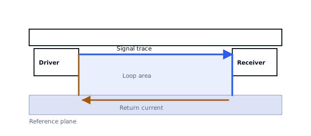
The loop, not the trace, is the circuit
Draw the outgoing trace. Draw the path the return takes. The shape enclosed between them is the circuit loop, and almost everything that matters is a property of that shape rather than of either conductor on its own.
Loop inductance grows with enclosed area. A long thin loop has more inductance than a short fat one. Inductance is what turns a fast current change into a voltage you did not want, through the familiar V = L · di/dt.
Radiated emission from a current loop grows with its area. A loop carrying alternating current is a small magnetic antenna, and its effectiveness depends on the area it encloses. Keeping the return underneath the signal is what makes that area small.
Susceptibility works the same way in reverse. The same loop that radiates also picks up. An external field induces a voltage proportional to the enclosed area.
Crosstalk between two signals depends on how much their loops share space. Two traces side by side over a solid plane each have a tight loop and couple weakly. The same two traces over a broken plane have large, overlapping loops and couple strongly.
Four different problems, one geometric cause. That is why return current is worth understanding once rather than memorising four sets of rules.
The phrase that gets it wrong
"Current takes the path of least resistance" is repeated constantly, and it is wrong in a way that matters here.
Current takes all available paths, dividing between them in inverse proportion to their impedance. Not resistance. Impedance.
At DC, impedance is resistance, and the phrase happens to give the right answer: the return spreads out across the plane and takes the most direct geometric route back, because that is the lowest-resistance route.
Above a few tens of kilohertz the inductive term dominates, and the lowest impedance path is the one that encloses the smallest loop, which is the copper directly beneath the trace. The current concentrates there, in a band roughly centred under the trace, even if that route is geometrically longer than cutting straight across the plane.
Texas Instruments makes an even finer distinction worth keeping: the mechanism is the path of least inductance specifically, rather than impedance in general. In practice both phrasings lead you to the same layout decisions, and both are better than the resistance version, which leads you to the wrong one.
Lesson 3 takes the frequency dependence apart properly. The point to carry away here is that "least resistance" is not a simplification of the truth. It predicts a different path.
Why the return concentrates under the trace
Two mechanisms, pulling the same way.
The trace and the plane beneath it form a loop. Return current flowing directly under the trace makes that loop as small as geometry allows, which makes its inductance as low as geometry allows. Current distributes itself to minimise the total energy stored in the magnetic field, and that minimum is the tight loop.
At the same time the trace and the plane form a capacitor, distributed along the length of the route. At high frequency that capacitance is part of how the signal propagates, and it ties the return to the region directly below.
The practical consequence is worth stating plainly, because it surprises people: if you route a trace in a loose S-shape across a board, the return current follows the S. It does not cut the corner. The copper under the trace is the low-inductance path at every point along the route, so that is where the current goes.
What this immediately tells you
Several layout rules that are usually taught separately turn out to be the same rule.
- Keep a solid plane adjacent to signal layers. You are providing a
low-inductance return directly under every trace.
- Do not route over gaps in the plane. You are forcing the return to
detour, which enlarges the loop.
- Put a return via near a signal via. When the signal changes reference
layer, the return needs somewhere to change with it.
- Keep high-speed traces short. Shorter trace, shorter loop.
- Route differential pairs tightly. Each line is largely the other's
return.
None of these is a convention. Each one is the same statement about loop area, seen from a different angle.
It is the same loop as decoupling
If you took the power integrity course, this will feel familiar, because it is the same geometry, and the lesson on loop inductance there is this one seen from the power side. A decoupling capacitor works by providing a small loop between the capacitor and the device pins for transient current. The lesson on loop inductance there and this lesson here are describing one phenomenon in two contexts.
The connection is worth making deliberately. A board with excellent decoupling and a broken reference plane has solved half the problem. The transient current has a tight loop at the device and then has to get back to the regulator, and if that return is interrupted the rail still moves.
A test you can run on any layout
Pick the fastest signal on the board. Put your finger on the driver pin. Follow the trace to the receiver. Now follow the return back, staying on the adjacent reference layer, directly beneath the trace, and see whether you can get all the way home without lifting your finger off copper.
Where you cannot, something had to give. Either the current found a longer way around, or it jumped layers through a via that may or may not be nearby, or it coupled through a capacitor you did not intend.
That walk takes about a minute per net and finds most grounding problems before they become EMC problems.
What comes next
Lesson 3 explains why the answer to "where does the return go?" is different at DC and at 100 MHz on the same board with the same copper, and why the number that decides it is the edge rate rather than the clock frequency.
Sources and further reading
- Texas Instruments: PCB design and return current guidance (SLYP173) — least inductance rather than least impedance, and the consequences of interrupting the return.
- Altium: What Is the Electrical Return Path in a PCB? — current distribution under a trace and its frequency dependence.
- All About Circuits: using return paths in PCB design — the path of least impedance framing and its layout consequences.
- Clemson Vehicular Electronics Laboratory: return paths and EMI — measured behaviour of return structures.