
Why High-Frequency Return Current Does Not Follow the DC Path
The same copper carries two different currents by two different routes.
- Lesson 3 of 10
- Intermediate
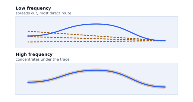
Here is a result that sounds like a contradiction. Take one board, one trace, one solid plane underneath. Send a slow signal: the return current spreads across the plane and takes a broad, direct route back. Send a fast signal down the same trace: the return current collects into a narrow band directly beneath it.
Same copper. Same geometry. Two different paths, because the current is choosing on a different criterion.
Quick answer. At low frequency the return path is set by resistance, so current spreads out and takes the most direct route across the plane. As frequency rises the inductive term grows and soon dominates, and the lowest impedance route becomes the one enclosing the smallest loop: directly under the trace. The crossover for a typical plane sits in the tens of kilohertz, so for anything digital the high-frequency behaviour is the one that applies.
The two terms
The impedance of a return path has a resistive part and an inductive part.
The resistance of a wide copper plane is very low and does not change with frequency in the range we care about. The inductive reactance is 2πfL: zero at DC, and growing in direct proportion to frequency.
At some frequency the second term overtakes the first. Below it, current distributes to minimise I²R, which means spreading out and going directly. Above it, current distributes to minimise stored magnetic energy, which means collapsing into the tightest available loop.
For ordinary PCB geometry, that crossover lands somewhere in the region of tens of kilohertz. The exact number depends on the trace height above the plane, the copper weight and the width of the return region, so treat it as an order of magnitude rather than a threshold to design against.
The useful conclusion from that number is blunt: for digital work, the low-frequency case is almost never the one you are in. Audio, DC distribution and precision instrumentation live below the crossover. Clocks, data lines, switching edges and anything with a sharp transition live far above it.
Why the clock frequency is the wrong number
A 10 MHz clock does not contain only 10 MHz. A trapezoidal waveform contains the fundamental and a series of harmonics, and how far that series extends is set by how fast the edges are, not by how often they repeat.
A 10 MHz clock with 1 ns edges carries meaningful energy up to hundreds of megahertz. A 100 MHz clock with deliberately slowed 5 ns edges may carry less high-frequency content than the slower one. The repetition rate tells you where the spectral lines sit. The edge rate tells you how far up they go.
This is why a board full of slow logic can fail EMC. A microcontroller toggling a pin at 1 kHz is a low-frequency signal by any reasonable description, and if that pin has a 2 ns edge then every transition injects energy into the hundreds of megahertz. The return current for those edges behaves like a high-frequency return, regardless of what the datasheet says about the clock.
When you are deciding whether a trace needs a clean reference, look at the edge rate in the logic family's datasheet and not at the bus speed.
Putting a number on the edge
A widely used estimate in high-speed design puts the upper end of the significant spectrum near 0.35 / t_r, where t_r is the 10 % to 90 % rise time. It is an approximation with assumptions behind it, not a law, and different authors quote slightly different constants. Used as what it is, an order-of-magnitude guide, it is enough to settle most layout arguments.
| Rise time | Approximate significant bandwidth |
|---|---|
| 10 ns | around 35 MHz |
| 5 ns | around 70 MHz |
| 2 ns | around 175 MHz |
| 1 ns | around 350 MHz |
| 500 ps | around 700 MHz |
Read the second column as the frequency up to which the return path has to behave itself. A general-purpose output on a modern microcontroller is commonly in the 2 ns to 5 ns region even when configured for a slow data rate, which puts it firmly in the hundreds of megahertz.
Two things follow. A board with no clock faster than a few megahertz can still need continuous reference copper. And slowing an edge deliberately, where the timing allows, moves the whole column down.
Both currents at once
The two behaviours are not alternatives. A real signal has a DC component, a low-frequency envelope and high-frequency edge content, and each part of the spectrum finds its own path through the same copper simultaneously.
A power rail feeding a digital device is the clearest case. The steady current spreads through the plane, taking the widest, most direct route. The transient current demanded at each clock edge takes the tight loop through the nearest decoupling capacitor. One conductor, one net, two current distributions superimposed, each behaving according to the frequency of the component that produced it.
This superposition is why plane geometry can be fine for power delivery and bad for signals at the same time. They are not using the plane the same way.
What this changes in practice
Where the plane matters is directly under fast traces. Copper elsewhere on the layer helps with heat and with DC. It does nothing for the return path of a signal it does not sit beneath.
A gap matters in proportion to the frequency crossing it. A slot under a slow analog line is largely harmless. The same slot under a fast differential pair is the defect in lesson 7.
Slowing an edge is a real tool. If a signal does not need a fast edge, series termination or a slower drive setting reduces its high-frequency content, which reduces what its return path can couple into. It costs timing margin, so it is a trade and not a free fix, but it is a legitimate one.
Measuring at the clock frequency can mislead you. Emissions usually show up at harmonics well above the fundamental, which is where the edge energy lives.
The connection to loop inductance
If you have worked through the power integrity course, the quantity governing all of this is the same one that governed decoupling: loop inductance, set by loop area and nothing else of comparable importance.
The difference is only which loop. There, it was the loop between the capacitor and the device. Here, it is the loop between the signal trace and its return. The mechanism, the arithmetic and the reason distance hurts are identical.
What comes next
With the frequency behaviour established, the next lesson takes on the grounding question that generates more bad advice than any other: whether to split analog and digital grounds, and what those two pins on a converter actually mean.
Sources and further reading
- Texas Instruments: PCB design and return current guidance (SLYP173) — frequency dependence of the return path and the least-inductance framing.
- Altium: What Is the Electrical Return Path in a PCB? — current distribution under a trace at low and high frequency, and why edge rate matters.
- All About Circuits: return paths and impedance — the transition between resistance-dominated and inductance-dominated behaviour.