
Why a Switching Regulator Oscillates
Phase margin explained without a control theory course.
- Lesson 10 of 10
- Intermediate
A regulator that oscillates is not broken in the way a shorted part is broken. Every component is within specification and the schematic is correct. What has gone wrong is a property of the whole loop, and you cannot see it by looking at any single piece.
This lesson explains enough control theory to diagnose that, and stops there.
Quick answer. A switching regulator measures its output, compares it to a reference and corrects. That correction takes time, and the output filter adds delay of its own. If the total delay reaches half a cycle at the frequency where the loop still has gain, the correction arrives in phase with the error and reinforces it. Phase margin is how much delay you have left before that happens, and a common target is 45 degrees or more.
The loop
Four things in a ring:
- The power stage converts a control signal into an output voltage.
- The output filter, the inductor and capacitor, smooths it and
introduces phase lag.
- The feedback divider scales the output for comparison.
- The error amplifier and compensation compare it to a reference and
produce the control signal.
Loop gain is what happens to a small disturbance after going all the way round. If the loop returns something smaller than it started with, the disturbance dies out. If it returns something the same size or larger, and in phase, it sustains or grows, and that is oscillation.
Gain and phase, and why both matter
Two quantities describe the loop at each frequency: how much it multiplies a signal, and how much it delays it.
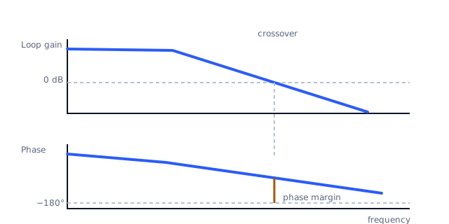
At low frequency the gain is high, which is what makes regulation accurate. As frequency rises the gain falls, and at some point it passes through 1, meaning 0 dB. That is the crossover frequency, and it is where stability is decided, because it is the highest frequency at which the loop can still sustain anything.
Meanwhile the loop adds phase lag. A feedback loop inverts by design, which is 180 degrees. The output filter adds more. If the extra lag reaches another 180 degrees at the crossover frequency, the total is 360, the feedback has become positive, and the loop sustains oscillation.
Phase margin is how far short of that you are at crossover. 60 degrees of phase margin means there is 60 degrees of additional lag available before trouble.
What the numbers mean in practice
| Phase margin | Behaviour |
|---|---|
| Below about 30° | pronounced ringing, long settling, close to the edge |
| 45° | the classic design target, slight overshoot, no ringing |
| 60° | well damped, clean transient response |
| Very high | stable but sluggish, slow to correct |
Texas Instruments' control loop material describes 45 degrees as giving good response with a little overshoot and no ringing, and treats 45 degrees or more as the design goal. Analog Devices frames it as a band, considering margins below roughly 40 degrees unstable and describing 40 to 70 degrees as the useful range.
Both agree on the region. The disagreement is about where exactly to put the line, which is a reminder that these are engineering targets rather than physical constants.
Gain margin is the companion figure: how much the gain could rise before reaching 0 dB at the frequency where the phase has already reached the critical value. It matters because gain varies with operating point, and a loop with good phase margin but little gain margin can misbehave when conditions change.
Where to put crossover
Higher crossover means faster response to load steps, because the loop reacts sooner. It also means the loop is still active closer to the switching frequency, where the switching ripple itself can be mistaken for signal.
Sources differ on the limit. Texas Instruments gives a rule of thumb of one fifth to one tenth of the switching frequency. Analog Devices recommends no more than one tenth. The conservative figure is the tenth, and the honest reading is that between fsw/10 and fsw/5 you are trading response speed for noise immunity, with the upper part of that range demanding more care.
For the running example at 500 kHz:
fsw / 10 = 50 kHz fsw / 5 = 100 kHz
So a crossover somewhere between 50 kHz and 100 kHz, with 50 kHz the safer starting point.
Poles, zeros and the output filter
Two terms, used plainly.
A pole makes gain start falling and adds up to 90 degrees of lag. A zero makes gain start rising and adds up to 90 degrees of lead, which recovers phase.
The output LC filter contributes a double pole, so up to 180 degrees of lag, at a frequency set by the inductor and capacitor. That alone is the whole phase budget, which is why compensation exists: it adds zeros that recover phase around the crossover region.
The ESR of the output capacitor also contributes a zero. On designs built around electrolytic capacitors that zero was part of the stability plan, which is why swapping to all-ceramic output capacitance can destabilise an old design. It removes a zero the compensation was counting on.
This is the mechanism behind the warning in lesson 7: adding output capacitance is not automatically safer. It moves the filter pole lower, which changes the phase at crossover, and whether that helps depends on where the compensation put its zeros.
Internally and externally compensated parts
The distinction decides how much of this is your problem.
Internally compensated devices have the compensation network on the die. The manufacturer chose it for a defined range of output capacitance and inductance, which is why the datasheet gives a range rather than a minimum. Your job is to stay inside the specified component ranges, and the stability work has been done for you within those bounds. Going outside them is where designs get into trouble, and the symptom is not an error message, it is ringing.
Externally compensated controllers bring the error amplifier output to a pin and expect you to build the network. You get control over crossover and margin, and responsibility for them. The device's datasheet gives a design procedure, and that procedure is the authority for that part.
In both cases the manufacturer's stated requirements take precedence over anything general. A rule of thumb that contradicts the datasheet of the part in front of you loses.
How to tell whether yours is stable
Without a frequency response analyser, three practical tests:
Load step response. Apply a step and watch the output. A clean overshoot that settles in a cycle or two suggests healthy margin. Several cycles of ringing suggests marginal phase margin. Sustained oscillation is unambiguous.
Vary the operating point. Stability can depend on input voltage and load. A loop that looks fine at nominal and rings at light load or high input is marginal rather than stable.
Look at the switching waveform. Pulse width jitter or alternating wide and narrow pulses often indicates loop trouble rather than a measurement artefact.
Where it matters, measuring loop gain directly with an injection transformer and a network analyser is the real answer, and it is routine practice on designs where the consequences justify the setup time.
Where this course ends
Ten lessons, one habit: follow the current, and then ask what the loop around it does. The topology decides where the current goes, the components decide how much, the layout decides what that current couples into, and the control loop decides whether the whole arrangement settles.
A datasheet will give you values for all of it. What it cannot give you is the reason, and the reason is what you need the day the standard arrangement does not fit.
Sources and further reading
- Texas Instruments: Control Loop Cookbook (SLUP113) — seminar paper, phase margin targets and loop shaping.
- Texas Instruments: Power Supply Design Seminar, compensation (SLUP340) — seminar paper, crossover frequency guidance and compensation design.
- Analog Devices: Power Supply Design, How Bode Plots Can Help — technical article, phase margin ranges and crossover recommendation.
- Texas Instruments: LM60430 / LM60440 datasheet — datasheet, internally compensated device with a specified output capacitance range.