
The Feedback Node: Quiet, High Impedance, Easy to Ruin
A few megohms of divider, a few millivolts of reference, and a switching node nearby.
- Lesson 8 of 10
- Intermediate
The feedback divider is two resistors. It is the cheapest part of the converter and the one that decides what the output voltage actually is, because the regulator does not know the output voltage. It knows the voltage on its feedback pin, and it adjusts until that matches its internal reference.
Anything that adds a millivolt to the feedback node is a millivolt of output error, or worse, a disturbance the loop will faithfully try to correct.
Quick answer. Keep the divider close to the regulator's feedback pin, route the feedback trace away from the switch node and the inductor, sense the output at the point you actually care about, and return the divider's ground to the device's quiet ground reference rather than to power ground. The node is high impedance, so it picks up capacitively, and the aggressor is a few millimetres away.
Why this node is fragile
Divider resistors are usually chosen in the tens to hundreds of kilohms, to avoid wasting current in a circuit whose purpose is efficiency. A 100 kΩ upper resistor and 100 kΩ lower gives a source impedance at the feedback node in the tens of kilohms.
High impedance means small injected currents become meaningful voltages. A capacitive coupling of a fraction of a picofarad from the switch node, which is swinging the full input voltage in nanoseconds, is enough to inject a disturbance that matters at a node whose reference is typically under a volt.
Lower resistor values reduce the impedance and the sensitivity, at the cost of quiescent current. On a battery product that trade matters; on a mains-fed board it usually does not, and lower values are the easier choice. Some devices specify a maximum divider impedance, which settles it.
The four decisions
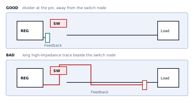
Where the divider sits. Next to the regulator, with the feedback trace from the divider's midpoint to the pin as short as possible. The long trace should be the one from the output to the top of the divider, which is a low-impedance node, not the one from the divider to the pin, which is not.
Placing the divider out at the load and running a long high-impedance trace back is the common version of this mistake. It feels like better sensing. It is a long antenna connected to the most sensitive pin on the device.
What it is routed away from. The switch node and the inductor body are the aggressors. Keep the feedback trace off any layer directly above or below the switch node copper, and out from under the inductor, which has a fringing field that does not respect the keepout you drew on the top layer.
Where the feedback trace has to pass near something noisy, a ground trace between them helps, and so does putting the feedback route on a layer with continuous reference copper between it and the aggressor. The grounding course covers why that reference has to be continuous to do anything.
Where it senses. The divider's top connects to the output. Which point of the output is a real choice, because the copper between the regulator and the load has resistance, and at 2 A even a few milliohms is millivolts of drop.
Sensing at the regulator gives a well-regulated voltage at the regulator and a slightly low one at the load. Sensing at the load corrects for the drop but lengthens the sense path and includes any noise picked up along the way. Where accuracy at the load matters, a Kelvin connection from the load point, routed as a quiet pair with its own ground reference, is the standard answer. Where it does not, sensing locally is simpler and more robust.
Where its ground returns. The bottom of the divider is a reference, and it must return to the device's analog or quiet ground, at the pin the datasheet nominates, not to the nearest convenient power ground copper.
This is the one that produces mysterious output voltage errors. The hot loop from lesson 6 is pushing amps of pulsed current through power ground. Any voltage developed across that copper appears directly in series with your reference if the divider's ground shares it. The device's own ground arrangement, as specified in its datasheet, exists precisely to keep those separate.
The feed-forward capacitor
A small capacitor across the upper divider resistor is common, and its purpose is loop compensation rather than filtering: it adds a zero that can improve phase margin and transient response.
It is device-specific. Some datasheets specify a value or a range and some explicitly recommend against one. Adding one because another design had one is how a stable converter becomes a ringing one, and removing one that the compensation assumed is how it becomes unstable. Lesson 10 explains what the zero actually does.
The honest guidance is: fit what the device's datasheet specifies for your output voltage, and if you want to change it, measure the loop.
What good and bad look like
Bad, and common:
- Divider at the load, long high-impedance trace back to the pin.
- Feedback trace running parallel to the switch node for several
millimetres.
- Divider ground tied to the nearest power ground pour, which happens to be
the input capacitor's return.
- A feed-forward capacitor copied from a different device's reference
design.
Good:
- Divider within a few millimetres of the pin, short trace to it.
- Feedback route kept away from the switch node and the inductor, with
continuous reference copper under it.
- Divider ground returned to the device's designated quiet ground point.
- Sense point chosen deliberately, and documented as a decision.
How to find the problem if you have it
A feedback layout problem usually shows as output voltage that is slightly wrong, or jitter on the switching waveform, or an output that moves when something else on the board switches.
The quickest discriminating test is to compare behaviour at light and heavy load. Coupling into the feedback node tends to scale with the switching activity, so a disturbance that grows with load and disappears at no load points at the layout rather than at the divider values.
What comes next
Lesson 9 goes to the aggressor itself: the switch node, why it couples so effectively, and why making it as small as possible is not quite the right instruction.
Sources and further reading
- Texas Instruments: LM60430 / LM60440 datasheet — datasheet, feedback divider placement, routing and ground reference guidance.
- Texas Instruments: LMS3655 datasheet — datasheet, feedback network layout and sense point selection.
- Texas Instruments: Control Loop Cookbook (SLUP113) — seminar paper, the role of the feed-forward zero in loop shaping.