
What Happens When a Signal Crosses a Plane Split
The trace crosses in a straight line. The return current does not.
- Lesson 7 of 10
- Intermediate
This is the failure the rest of the course has been building towards, and it is worth following one step at a time, because every step is ordinary and the result is not.
A board has a split in its ground plane. Someone routes a signal across it. Nothing in the design rule check objects. The board assembles, powers up and works on the bench.
Then it fails EMC at 240 MHz, and the trace that caused it looks exactly like every other trace on the board.
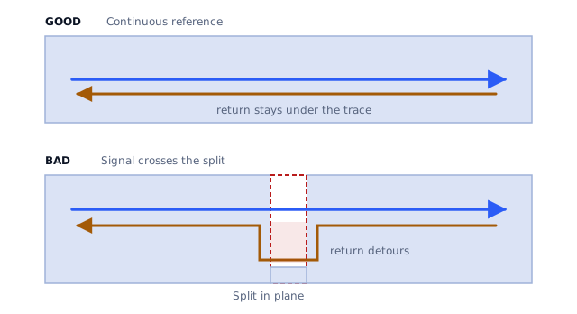
Quick answer. The signal crosses the gap through its own trace. Its return current cannot, because there is no copper under the trace at the gap. The return runs along the edge of the split to wherever the two regions connect, crosses there, and comes back along the other edge. Signal and return now enclose a loop as large as that detour, which raises inductance, distorts the edge and turns the gap into an efficient radiator.
Step by step
Before the gap. The signal travels on the top layer. Its return travels in the plane directly beneath it, a fraction of a millimetre away. The loop is tiny and the inductance per unit length is low and constant. This is a transmission line and it behaves like one.
At the gap. The copper under the trace ends. The return current arrives at the edge of the split and has nowhere to go.
The detour. It does not stop, because current cannot stop. It flows along the edge of the gap, looking for a connection to the other region. It finds one wherever the designer put one, which might be a bridge somewhere along the split, a connection at the power supply, or in the worst case a path through another layer entirely.
Crossing. It crosses there, then runs back along the far edge of the gap until it is underneath the trace again.
After the gap. Normal service resumes, as though nothing happened. The transmission line continues.
Four consequences
The loop area jumps. The loop enclosed by the signal and its return was a thin sliver following the trace. Now it includes the whole detour. If the split is 40 mm long and the bridge is at one end, the loop has gained something in the order of tens of square millimetres at the point of crossing.
The impedance changes abruptly. A transmission line's impedance depends on the geometry between conductor and reference. At the gap that geometry changes completely over a very short distance. The signal sees a discontinuity and part of it reflects, which shows up as ringing, overshoot and degraded timing margin.
The structure radiates. A loop carrying high-frequency current radiates in proportion to its area. The detour loop is large and it carries the full high-frequency content of the signal's edges. The gap itself, now with a voltage developed along it, behaves as a slot driven at its edges, which is an efficient radiating structure at frequencies where the slot is a meaningful fraction of a wavelength.
Everything else crossing the gap couples. Two signals crossing the same split share the same detour path. Their return currents flow through common impedance, which couples them to each other directly. This is the crosstalk that appears between nets with no physical proximity, and it is confusing until you look at the returns.
Why the bench does not catch it
The signal arrives. Logic thresholds have margin, and the ringing introduced by one discontinuity usually does not break functionality on a short board at moderate speed.
What has changed is the emission profile and the coupling, and neither is visible without the right instrument. A scope probe on the receiver shows a slightly uglier edge. You have to be looking for it to see it, and you have to know what the edge looked like before.
This is the core reason reference discontinuities deserve attention at layout time rather than at debug time: the board works, so nothing prompts the investigation until a test lab prompts it.
How to find them before the lab does
Look at the plane layer alone. As in lesson 1. A split is obvious when nothing else is on screen.
Then look at the signal layers over it. Most tools can show two layers at once. Any trace crossing the gap is a candidate.
Check the layer below as well as above. A plane sits between two signal layers and references both. A split affects traces on either side.
Pay attention to accidental splits. A deliberate moat is at least deliberate. A row of connector anti-pads, a trace routed across the plane layer or a long thermal relief chain is a split nobody decided on, and it is the common case.
If a signal has to cross
Sometimes the split is required, usually for isolation, and something has to get to the other side. In rough order of preference:
- Do not cross. Reroute the signal to stay on one side. Most of the time
this is possible and simply takes effort.
- Cross at a deliberate bridge. If a region of continuous copper joins
the two sides, route every crossing signal over that bridge, together. The return follows the signal across the bridge and the loop stays small.
- Give the return a local path. Where the gap separates two different
nets rather than two parts of the same one, a capacitor across the gap next to the crossing gives high-frequency return a route. It is better than nothing and worse than not crossing.
- Cross with something slow. If one of the signals must cross, make it
the slowest one. An I²C line at 100 kHz with a soft edge crossing a gap is a much smaller problem than a clock.
- Cross through an isolator. For a genuine isolation barrier this is the
only correct answer, and the barrier exists precisely so that no galvanic path crosses.
Note what is not on the list: a ferrite bead bridging the gap under the crossing signal. It is an inductance deliberately placed in a return path, and it makes the detour worse while feeling like a fix.
The general rule, stated carefully
A trace needs continuous reference copper directly beneath it, from driver to receiver, on the layer adjacent to it, for its whole length. Where that continuity is interrupted, the return current detours and the loop grows by the size of the detour.
That is the whole of it. Everything else in this course is an application of that sentence to a particular situation.
What comes next
Lesson 8 takes a complete mixed-signal board and applies all of this: a sensor, an analog front end, a converter, a microcontroller and a supply, with each placement and plane decision justified by where the current goes.
Sources and further reading
- Texas Instruments: PCB design and return paths (SLYP173) — consequences of interrupting the return path under a trace.
- Altium: return current and obstacles in the plane — how the return finds its way around a discontinuity.
- Autodesk summary of Henry Ott's mixed-signal partitioning guidance — why routing across a split enlarges the return loop and raises radiation.
- Clemson Vehicular Electronics Laboratory: discontinuities as EMI sources — excitation of board structures by return path interruptions.