
Grounding a Mixed-Signal Board, Step by Step
One sensor, one converter, one microcontroller, and every decision justified.
- Lesson 8 of 10
- Intermediate
Principles are easy to agree with and hard to apply, so this lesson takes one board and makes every grounding decision on it, with the reason attached.
The board is invented for the purpose. It is deliberately ordinary, because the interesting part is the reasoning and not the novelty.
The board
A four-layer instrument board, roughly 70 mm by 50 mm:
- A bridge sensor producing a few millivolts, connected through a short
shielded cable to a connector at one edge.
- An instrumentation amplifier and a second-order filter.
- A 16-bit SAR converter with a serial interface, with its own reference.
- A microcontroller reading the converter and driving a USB interface.
- A switching regulator producing the digital rail from an external supply,
and a linear regulator producing the analog rail from it.
Stackup, decided before anything else: signal, ground, power, signal. One continuous ground plane on layer 2, under everything.
Placement, which is where grounding is decided
Placement is the grounding design. Everything after it is bookkeeping.
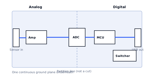
Draw the partition first. A line across the board, analog on the left, digital on the right. It is a line in your head and in the placement, not in the copper.
Connectors at opposite ends. The sensor connector at the far left edge, the USB connector at the far right. The sensor's return current has no reason to travel through the digital half, and the USB return has no reason to travel through the analog half, because neither connector is anywhere near the other half.
The converter sits on the partition. Analog pins facing left, digital pins facing right. This is the single most consequential placement on the board. Rotate it 180 degrees and the serial interface traces have to cross the analog region to reach the microcontroller, dragging digital return current across it.
The switching regulator goes in the far corner of the digital half. Its switching loop is the noisiest current loop on the board. The distance is not to keep it away in general, it is to keep its return loop geographically separate from the analog reference region.
The linear regulator for the analog rail sits near the analog section, at the boundary, fed from the digital side. It is the deliberate crossing point for supply current, and a linear regulator with reasonable rejection is a good place for the handover.
The plane
One continuous ground plane on layer 2, unbroken across the whole board.
No moat. No split under the converter. No bridge. The separation comes from the placement: the digital traces are all on the right half, so the digital return currents flow in the right half, because return current flows directly under its trace. There is nothing to carry them left.
This is the partitioning approach that Henry Ott advocates and that Texas Instruments' applications material arrives at as well. It works on exactly one condition, which is the condition in the next section.
Routing, where the design gets thrown away
Partitioning fails through routing, every time. Three rules, and the third is the one that gets broken:
- Analog signals stay in the analog half.
- Digital signals stay in the digital half.
- No digital signal takes a shortcut across the analog half, ever, not
even one, not even a slow one, not even for 5 mm because the autorouter found a nice gap.
A single SPI clock routed diagonally across the analog section puts its return current directly under the amplifier, which is the exact situation the whole arrangement was built to prevent. There is no copper feature protecting you from this. It is a discipline, and it needs checking rather than trusting.
The converter's serial interface is the one set of signals that genuinely crosses the partition line, and it crosses at the converter, which is on the line. Those traces run to the right, into the digital half, and stay there.
The converter's two ground pins
The converter has AGND and DGND. Following the reasoning in lesson 4 and the guidance from Analog Devices for a converter of this size, both pins connect to the single ground plane, at the device, with short connections.
The digital supply pin of the converter is decoupled to its DGND pin with a small capacitor placed as close to the pins as the footprint allows, so that the converter's own internal digital switching current circulates in a loop a couple of millimetres across rather than out into the board. That loop is the one that matters for the converter's own performance, and its size is set by the placement of that one capacitor.
The analog supply gets its own decoupling to AGND, equally close. How those capacitors behave as a system is the subject of the power distribution network lesson in the power integrity course.
The reference
The converter's voltage reference deserves separate thought, because a 16-bit conversion is a comparison against it. Noise on the reference is indistinguishable from noise on the signal.
The reference device goes close to the converter, inside the analog region, with its own decoupling and a short, direct connection to the converter's reference pin. Its ground connection goes to the plane right there, next to the converter's analog ground pins, so that the reference and the converter share the same piece of copper rather than two ends of a current path.
Where the digital return current actually goes
Worth tracing explicitly, because this is the claim the design rests on.
The microcontroller switches a pin. Current leaves the pin, travels along the trace towards the converter, and the return flows in the plane directly beneath that trace. The trace is in the digital half, so the return is in the digital half. At the converter, which sits on the boundary, the current turns around. The deepest it penetrates towards the analog side is the width of the converter package.
The USB interface current loops between the microcontroller and the connector, both on the right edge. It never comes near the amplifier.
The switching regulator's loop is in the far corner, and its return current has no reason to travel left because its load is on the right.
No slot in the copper was required for any of that. The currents are separated because the things that produce them are separated.
What would make this board need a split
In honesty, something might. If the digital section grew into a processor pulling hundreds of milliamps in transients, or if the converter were a 24-bit device looking for sub-microvolt stability, the situation changes, and Analog Devices draws exactly that distinction for large digital devices with integrated analog.
At that point the right move is to read the manufacturer's layout guidance for that specific device and follow it, including the placement that goes with it. It is not to invent a split because the board feels complicated.
The review
Before release, four questions:
- Does any digital trace enter the analog half? Check visually, layer by
layer, not by DRC.
- Is the ground plane continuous under every signal on the board?
- Are the converter's decoupling capacitors within a couple of millimetres of
the pins they serve?
- Does the switching regulator's return current have any reason to travel
towards the analog section?
If all four answers are good, the grounding on this board is done, and no copper was cut to achieve it.
What comes next
Lesson 9 follows the current off the board entirely, into the connector and the cable, which is where a carefully controlled return path usually stops being controlled.
Sources and further reading
- James Bryant, Analog Devices: Grounding Analog-Digital Converters — converter ground pin treatment, decoupling to DGND, and the large-device exception.
- Analog Devices MT-031: Grounding Data Converters — the same reasoning with layout figures.
- Texas Instruments Analog Applications Journal: mixed-signal grounding (SLYT512) — single plane with partitioning and the routing discipline required.
- Autodesk summary of Henry Ott's partitioning method — partition, route within sections, place the converter on the boundary.