
Connectors: What Happens When the Signal Leaves the Board
Your careful return path ends at the connector unless you continue it.
- Lesson 9 of 10
- Intermediate
Everything so far has assumed the current stays on the board. At a connector it does not. The signal leaves through a pin, travels down a cable, and has to come back through another pin, and the geometry that was under your control for the whole route is now determined by a pinout and a bundle of wire.
Connectors are where well-grounded boards go wrong, because the return path ends at the board edge unless someone continues it deliberately.
Quick answer. A connector interrupts the reference plane and forces the return current through specific pins. The loop between a signal pin and its nearest return pin, extended along the cable, sets the loop area for everything leaving the board. Return pins distributed next to their signals keep that loop small. A single ground pin in a corner makes one large loop shared by every signal, which is both a coupling path and an antenna feed.
The plane stops here
A connector footprint is a row of holes or pads, each with clearance in every plane it passes through. A 20-way header punches twenty clearances in a line, and the result is a slot, as lesson 1 described.
That slot sits exactly where the high-speed signals are heading, because they are heading for the connector. So the first connector problem is on the board, before any current reaches a pin: the reference under the approach to the connector is weakened by the footprint itself.
What helps:
- Tie the plane layers together with stitching vias close to the footprint, on
both sides of it, so the plane remains a single conductor around the interruption.
- Approach the connector from the direction with the most continuous copper
rather than across the row of anti-pads.
- Where the connector is on an edge, keep the plane continuous right up to
the footprint rather than pulling it back for clearance you do not need.
Pin assignment is loop geometry
Once the current reaches the pins, the pinout decides the loop.
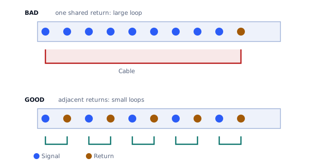
Take a ten-pin connector with nine signals and one ground pin at the end. Each signal's return must reach that one pin. The loop for the signal at the far end of the connector encloses the entire connector width plus the length of the cable. Every signal shares that one return pin and therefore shares its impedance, so they also couple into each other through it.
Now take the same connector with signals and returns alternating. Each signal's return is in the next pin along. The loop is a pin pitch wide. The same cable, the same board, several times less enclosed area and no shared return impedance between distant signals.
The measurement literature backs the intuition. Work from Missouri S&T on connector EMI examined the number and arrangement of ground pins and found emissions depending on them, and reported that for open pin field connectors emissions change inversely with the number of power and ground pins. The mechanism they describe is the one above: return current through the connector's transfer impedance develops a small voltage between the two grounds, and that voltage drives the attached structures as an antenna.
So the design question for a pinout is not "how many ground pins are enough" in the abstract. It is "where is the return for this particular signal, and how big is the loop that makes".
Practical pin rules
- Give fast signals an adjacent return. Not a return somewhere on the
connector. The next pin.
- Distribute grounds rather than grouping them. Four ground pins spread
through the connector are worth more than four in a block at one end.
- For differential pairs, keep the pair adjacent and give the pair a
neighbouring ground, so the pair's own coupling does the work and the ground handles the common-mode part.
- Separate noisy and sensitive signals within the connector, with returns
between them, for the same common-impedance reason as anywhere else.
- Check what the mating cable does. A beautiful alternating pinout
connected to a ribbon cable where all the grounds are commoned at the other end has lost half its benefit.
Cables and common-mode current
Inside the board, signal and return are a few tenths of a millimetre apart. In a cable they might be a few millimetres apart, and in a bundle of loose wires they might be anywhere.
The differential current, equal and opposite in signal and return, radiates little when the two conductors are close. The part that causes trouble is common-mode current: current flowing in the same direction on all conductors, returning through some other path entirely, often through the chassis or through stray capacitance to the surroundings.
Common-mode current on a cable is efficient at radiating, because the cable is long and there is no nearby return to cancel it. A small common-mode current on a long cable can dominate a board's emissions even when everything on the board is tidy.
Where does it come from? Mostly from a voltage difference developed between the board reference and the far end of the cable, which is exactly the ground shift that the connector's return impedance produces. Reduce that shift and you reduce the drive.
That gives a clear order of attack, from cause to symptom:
- Keep the return path tight through the connector, with adjacent return
pins, so less voltage develops in the first place.
- Keep the plane continuous and stitched around the connector.
- Use twisted or closely paired conductors in the cable so the differential
loop stays small outside the board.
- If a shield is present, terminate it properly at the connector rather than
through a length of wire to a pin. A shield connected by a short pigtail stops being a shield at the frequencies where you need it.
- Only then reach for a common-mode choke or a ferrite on the cable. These
work, and they are treating the symptom.
Chassis connections
Where a product has a metal enclosure, the relationship between board reference and chassis affects cable emissions, because the chassis is part of the structure the common-mode current flows through.
This gets specific to the product, the enclosure and the regulatory context quickly, and it overlaps with safety requirements when mains or protective earth are involved. That is outside the scope of this course. The bounded statement that is safe to make: the connection between board reference and chassis, and its location relative to the cable entry, is a design decision with EMC consequences, and it should be made deliberately and verified rather than inherited from a mechanical drawing.
Where protective earth, isolation or creepage and clearance are involved, the applicable safety standard governs, and nothing in a layout course overrides it.
Before you commit a pinout
A connector pinout is one of the hardest things to change later, because it propagates into cable assemblies, mating boards and documentation. Worth twenty minutes before it is frozen:
- For each fast signal, which pin is its return, and how far away is it?
- Is any single pin acting as the return for many signals?
- Does the plane stay continuous up to and around the footprint?
- What does the cable do with these pins at the other end?
- If there is a shield, how is it terminated, physically?
What comes next
Lesson 10 collects the whole course into a review you can run on a finished layout, in your PCB editor, before the files go to the fabricator.
Sources and further reading
- Missouri S&T: EMI characteristics of high-performance inter-PCB connectors — ground pin count and arrangement, signal pin designation and measured emissions.
- Howard Johnson: measuring connectors — ground transfer impedance, ground shift and why it drives radiating structures.
- In Compliance Magazine: grounds and returns — return conductors, loop area at system level and the behaviour of return lines as emission paths.
- Clemson Vehicular Electronics Laboratory: EMI from board and cable structures — excitation of attached structures by return path impedance.