
Ground Vias and Stitching Vias: Where and Why
A signal that changes layer needs its return to change layer too.
- Lesson 6 of 10
- Intermediate
A signal via is easy to think about. The trace needs to get from layer 1 to layer 4, so you place a via and the tool routes through it.
The return current also needs to get from the reference next to layer 1 to the reference next to layer 4. Nothing in your layout tool will tell you that, and nothing will place the via that lets it happen.
Quick answer. A return via, placed next to a signal via, gives the return current a short path between reference layers at the point where the signal changes layer. Without one, the return has to travel to wherever the nearest connection between those planes happens to be, enclosing a much larger loop. Stitching vias are the same idea applied along plane edges and around regions, tying copper together so return current always has a nearby route.
What a layer change does to the loop
While the signal runs on layer 1 over a plane on layer 2, the return flows in layer 2 directly beneath it. Small loop, nothing to think about.
At the via, the signal drops to layer 4, which references a different plane, say layer 3. The return current now has to appear in layer 3. It cannot get there by magic. It needs a conductive path between the two planes.
If the nearest connection between those planes is 30 mm away, the return current goes 30 mm there, crosses, and comes 30 mm back. You routed a via; the return routed a detour. The loop is now tens of millimetres across at the exact point where the signal is making its fastest transition.
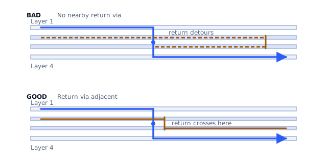
Put a ground via next to the signal via and the detour disappears. The return crosses where the signal crosses.
The case where a ground via is not enough
Everything above assumes both planes are ground. Often they are not.
If the signal goes from a layer referenced to ground onto a layer referenced to a power plane, a ground via cannot help, because the two planes are different nets. You cannot short them.
What you have instead is the capacitance between the two planes, which does carry high-frequency return current, and which is distributed across the whole board rather than concentrated where you need it. The usual remedies:
- Add a stitching capacitor between the two planes near the transition,
giving the return a local high-frequency path. It is a real improvement, and it is worse than a via because a capacitor has inductance of its own.
- Change the stackup so the signal keeps the same reference before and after.
- Reroute so the signal does not need that particular transition.
The order matters. Reference continuity through stackup is better than a component patching a discontinuity.
About spacing numbers
Ask how far a return via should be from its signal via and you will get a number. Ask three sources and you will get three numbers.
Here is the honest position: the right distance is as close as the footprint allows, and any specific figure you find is attached to a context. Texas Instruments gives a figure in the region of 200 mil centre to centre for ground stitching vias at signal transitions in one of its interface layout guides, which is a useful datum for that family of parts at those speeds. It is evidence about an interface standard, not a universal constant, and quoting it stripped of its origin is how rules of thumb get born.
The same applies to stitching a plane edge or a shielding fence. Guidance based on a fraction of a wavelength, commonly somewhere between a twentieth and a tenth of the guided wavelength at the highest frequency of interest, has a physical argument behind it. Using it requires knowing your highest significant frequency and the propagation velocity in your dielectric, which means it is a calculation and not a number.
So: place return vias adjacent to the transition, as close as clearance rules permit. Where a device's own layout guide gives a figure, use that figure. Do not carry it to the next project.
Where stitching vias earn their place
Beside every high-speed layer transition. The main case, covered above. The same reasoning governs where a decoupling capacitor goes, which the power integrity course treats as a question of placement.
Around the board edge, tying the plane layers together near the perimeter. This limits the edge from behaving as a radiating slot at high frequency and keeps the plane pair at a common potential around the outside.
Across large plane areas on multi-layer boards, so the two ground layers behave as one conductor rather than as a pair that can support a voltage difference between them.
Around connectors, where the return path has to be continuous right up to the point the current leaves the board. Lesson 9 goes into this.
Underneath and around a shielding can, where the can's effectiveness depends on its connection to the reference being continuous rather than at a few points.
Where they do nothing
Pouring copper on an unused outer layer and stitching it every 5 mm to the plane is a popular move, and mostly it is harmless. It does not improve the return path of a signal routed on an inner layer, because that signal's return is already in the adjacent plane. It is not a substitute for a reference plane and it does not compensate for a slot elsewhere.
There is also a cost to overdoing it. Every via is a hole through every plane it passes, and a dense field of vias in a small area removes enough copper that the plane itself becomes perforated. At that point you are solving one discontinuity by creating another.
A short review procedure
When the layout is done, take the fastest nets and check their transitions:
- For each signal via on a fast net, is there a ground via within a few
millimetres?
- Do the two layers the signal moves between reference the same net?
- If not, is there a stitching capacitor nearby, and is it the best available
answer rather than the first one?
- Around each connector, is the plane tied together close to the pins?
- Are there regions where vias are so dense that the plane has become a mesh?
The first question alone catches most of it, and most layout tools can show you every via on a net in a few seconds.
What comes next
Lesson 7 takes the failure that all of this is trying to avoid and follows it step by step: a signal crossing a split in its reference plane, and what happens to the return current, the signal and the emissions.
Sources and further reading
- Texas Instruments: interface layout guidance with device-specific stitching via placement — a worked figure for ground stitching vias at signal transitions, in its original context.
- Sierra Circuits: stitching vias — general purpose of stitching and plane tying.
- Clemson Vehicular Electronics Laboratory: return path discontinuities — why reference transitions excite board structures.