
Star Grounding: When It Helps and When It Makes Things Worse
A topology that solves a low-frequency problem, applied to a high-frequency one.
- Lesson 5 of 10
- Intermediate
Star grounding has a reputation problem in both directions. In one tradition it is the mark of a careful designer. In another it is the thing a junior engineer does to a high-speed board before the EMC lab explains otherwise.
Both reputations are earned, because the technique solves a specific problem and is often applied where that problem is not the one you have.
Quick answer. Star grounding gives each circuit its own return conductor back to one common point, so no circuit's return current flows through another circuit's return impedance. That solves conducted low-frequency coupling, which is a real problem in precision analog, audio and high-current designs. It does nothing useful above the frequency where inductance dominates, and on a fast digital board it makes return paths long, which is the opposite of what those signals need.
The problem it was invented for
Picture three circuits sharing one return conductor back to the supply: a power stage drawing an amp with a varying load, a microcontroller, and a precision amplifier working with millivolts.
That shared conductor has resistance. Small, but not zero. The power stage's varying current develops a varying voltage across it, following V = I · R. Every other circuit referenced to that conductor sees that voltage added to its own reference.
For the microcontroller this is irrelevant. For the amplifier it may be larger than the signal.
This is common-impedance coupling, and it is the problem star grounding exists to solve. Give each circuit its own return conductor back to a single common point, and no circuit's current flows through another's return impedance. The coupling is gone, because the shared element is gone.
Nothing about that reasoning is obsolete. Where the mechanism applies, the remedy still works.
Where it genuinely applies
The reasoning holds when the coupling is resistive and the frequencies are low enough that the inductance of the long individual returns does not matter. That describes a recognisable set of designs:
- Precision DC and low-frequency measurement, where microvolts of shift in a
reference are a real error.
- Audio, where the frequencies are low and the dynamic range is large.
- Power distribution within an enclosure, where high currents share
conductors with sensitive electronics.
- Rack and chassis wiring, where returns are physically long wires and their
resistance genuinely differs.
What these have in common is that the signals of interest sit below the frequency where the inductance of a long return path becomes the dominant term. Below that point, a long dedicated return is a good trade: you accept some inductance that does not matter in exchange for removing a resistance that does.
Where it stops working
Above that crossover the trade reverses, and it reverses hard.
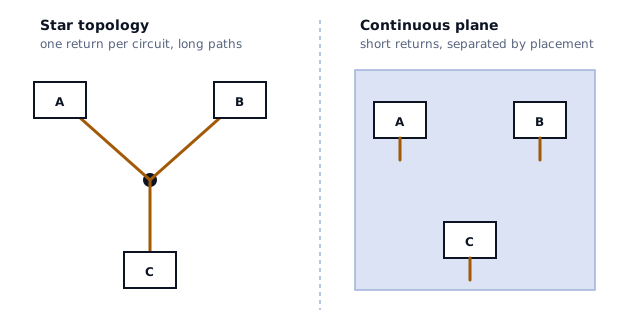
A star topology deliberately gives each circuit a long, individual return conductor. On a fast digital board, that is a long, individual, high-impedance return path, which is precisely the thing lessons 2 and 3 said to avoid.
Worse, implementing a star on a PCB usually means cutting the plane into regions so that the returns stay separate. Now every signal crossing between regions meets a reference discontinuity, and its return current goes the long way around to the star point. Large loops, by construction, in a design whose entire premise was control.
The failure is not that star grounding is wrong. It is that it optimises the resistive term while making the inductive term much worse, on a board where the inductive term is the one that matters.
The question that decides it
Not "is star grounding good practice?" but:
Is the coupling I am worried about resistive or inductive?
If the mechanism is shared resistance at low frequency, separating the returns helps. If the mechanism is loop area and mutual inductance at high frequency, separating the returns hurts, and a continuous plane with short returns helps.
Most real boards contain both. A motor driver and a precision sensor on the same board have a low-frequency common-impedance problem. The same board's SPI bus has a high-frequency loop problem. They want different things, which is why mixed boards are hard and why the answer is usually local rather than global.
What that looks like in practice
The useful compromise on most boards is a continuous plane with star-like current routing where it matters. You keep the plane for the benefit of every high-frequency return, and you arrange the high-current paths so their return does not flow through the sensitive section.
Concretely:
- Keep the plane continuous.
- Place the high-current stage so that its return reaches the supply without
passing under the sensitive circuitry. This is a placement decision, not a copper decision.
- Bring the high-current return to the supply input as its own route within
the plane, by keeping that current's loop geographically separate.
- Reference the sensitive analog section to a quiet area of the same plane,
physically away from the high-current loop.
You get the resistive separation from geography and the inductive benefit from continuity. The high-current return and the sensitive reference do not share copper in any meaningful way, because they are in different parts of the board, not because there is a slot between them.
Where a real split is still defensible
There are cases where a genuine break in copper is correct, and they share a feature: nothing crosses the gap.
- Galvanic isolation. An isolation barrier separates two circuits that do
not share a reference by design. The gap is the point, the clearance is a safety requirement, and signals cross only through the isolator.
- A separate reference that never carries signal across the boundary, such
as a guarded input region, where the only connections are deliberate.
The test is the same every time: identify every conductor crossing the gap and ask where its return goes. If the honest answer is "around the long way", the split is a mistake. If the honest answer is "nothing crosses", it is a design.
What comes next
Lesson 6 goes from topology to hardware: ground vias and stitching vias, where they do real work, and why a universal spacing number is not something anyone can honestly give you.
Sources and further reading
- James Bryant, Analog Devices: Grounding Analog-Digital Converters — the system star point, where it belongs, and why placing it at the converter is rarely right.
- Texas Instruments Analog Applications Journal: grounding and partitioning (SLYT512) — single-plane partitioning as the general case for mixed-signal boards.
- In Compliance Magazine: grounds and returns — common-impedance coupling and return conductors at system level.