
Switch Node Layout: Small, But Not At Any Price
The node with the fastest voltage edges on the board, and a thermal job to do.
- Lesson 9 of 10
- Intermediate
The switch node is the copper between the high-side switch, the low-side device and the inductor. In a 12 V converter it swings between roughly 12 V and roughly 0 V, and it does so in a few nanoseconds, half a million times a second.
It is the most electrically violent place on the board, and it has to be, because that is how the converter works. The design question is not how to make it calm. It is how to keep what it does contained.
Quick answer. Keep it compact, because its area sets how strongly it couples capacitively into everything nearby. But not at any price: the node also conducts the full inductor current and often carries heat away from the switching device, so shrinking it without limit trades a coupling problem for a thermal one. Compact, wide enough for the current, large enough for the heat, and away from anything sensitive.
Why it couples
A conductor carrying a rapidly changing voltage couples to its neighbours through the capacitance between them. The current injected is:
i = C · dv/dt
Both terms are large here. The capacitance between the switch node copper and an adjacent trace or plane is small, in the picofarad or sub-picofarad range, but dv/dt is enormous. Twelve volts in five nanoseconds is 2.4 × 10⁹ V/s.
Through just 1 pF that gives:
i = 1 × 10⁻¹² × 2.4 × 10⁹ = 2.4 mA
Two and a half milliamps injected into a neighbouring node, in a pulse, every switching cycle. Into a low-impedance node that is nothing. Into the high-impedance feedback node from lesson 8, it is a serious disturbance.
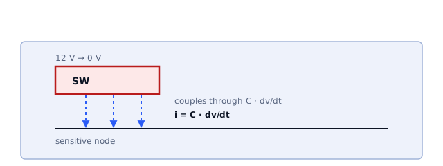
The coupling capacitance scales with the overlapping area and falls with separation. So the two controls you have are how much copper the node occupies and what is near it, including on adjacent layers.
Why smaller is better, up to a point
Reducing the switch node area reduces:
- Capacitive coupling to neighbouring traces and planes, as above.
- The area of the loop that the switching current traverses, which reduces
radiated emission for the same reason as lesson 6.
- The energy stored in the node's own capacitance, which is dissipated every
switching cycle, so a smaller node is marginally more efficient at high frequency.
This is the basis of the usual advice, and it is sound.
Why "as small as possible" is wrong
Three things pull the other way, and on real boards they matter.
Current. The node carries the full inductor current, 2 A in the running example and much more in bigger designs. Copper has to be wide enough to carry it without excessive heating and without adding resistance in a path that is already dissipating.
Heat. On many integrated regulators, the switch node copper is a deliberate thermal path. The datasheet's recommended layout often shows a specific copper area connected to that pin because the device sheds heat through it. Shrinking it to minimise coupling can push the die temperature up, trading an EMI margin you may have for a thermal margin you need.
Manufacturability. A node squeezed to the geometric minimum can create assembly problems and leaves no room for the vias that the thermal path needs.
So the instruction is not "minimise". It is: make it no larger than it needs to be for current and heat, and then control what sits near it. Where the datasheet specifies a copper area for thermal reasons, that specification wins, and the coupling is managed by keeping sensitive things away rather than by shrinking the node below what the device requires.
What to keep away from it
In rough order of how badly they react:
- The feedback trace and divider. Lesson 8.
- Any high-impedance analog node: references, sensor outputs, high-value
dividers.
- Reset and enable lines, which can glitch.
- Crystal and oscillator circuits.
- Communication buses, especially slower ones with long settling, which are
more easily disturbed than fast differential ones.
And in three dimensions, not two. A sensitive trace on the layer directly below the switch node is adjacent to it, however much clearance it has on its own layer. The usual arrangement puts a continuous ground plane immediately under the switch node, which both gives the switching current a tight return and shields what lies beneath. That return is the same return discussed in the grounding course, and interrupting it under the switch node is a straightforward way to make the problem worse.
The ringing on the node
Look at a switch node on a scope and you will usually see overshoot and ringing on each edge. It comes from the loop inductance of lesson 6 resonating with the device's output capacitance.
Two things are worth knowing about it:
- Its amplitude is a direct measure of how good your hot loop layout is. A
tight loop rings less. It is the cheapest layout quality metric you have.
- The ringing frequency is typically far above the switching frequency, in
the tens to hundreds of megahertz, which is exactly the range that shows up in radiated emissions testing.
If a design fails EMC in that range, the switch node waveform is the first place to look, and the fix is usually in the hot loop rather than in a filter added later. A snubber across the low-side device can damp it, at the cost of dissipating the energy it removes, and it is a legitimate tool once the layout is as good as it is going to get.
A short review for the node
- Is the node as compact as the current and thermal requirements allow?
- Does the datasheet specify a copper area for it? Is that respected?
- Is there continuous reference copper directly beneath it?
- Is anything sensitive routed above, below or beside it?
- Is the feedback trace anywhere near it?
- On a scope, how much does it overshoot and ring?
What comes next
Lesson 10 closes the course with the behaviour that ties all of this together: the control loop, and what makes a regulator stable, marginal or oscillating.
Sources and further reading
- Texas Instruments: LM60430 / LM60440 datasheet — datasheet, switch node layout and the thermal role of its copper.
- Texas Instruments: LMS3655 datasheet — datasheet, switch node area guidance alongside thermal requirements.
- Texas Instruments: Power Supply Design Seminar, switching loss mechanisms (SLUP340) — seminar paper, node capacitance and switching energy.
- Analog Devices: Buck Power Stage Design Equations — application note, power stage currents through the switch node.