
How to Drive a SAR ADC Correctly
The resistor and the capacitor at the input are not a filter. They are a settling budget.
- Lesson 6 of 6
- Advanced
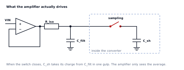
Almost every SAR converter datasheet shows a resistor and a capacitor between the amplifier and the input pin. Almost every design copies the values. Almost nobody can say what either of them is for.
They are not a filter. They happen to filter, and choosing them as if filtering were the point produces a circuit that measures a few codes wrong for a reason nobody can find.
Quick answer. The capacitor supplies the charge the converter takes at each sample, so the amplifier does not have to. The resistor isolates the amplifier from that capacitor so it stays stable. Three constraints size them: the array must settle during acquisition, the capacitor must recover before the next sample, and the resistor must not turn the average input current into a DC error. The third one usually binds, and it is the one that gets forgotten.
The three constraints
Take the converter this course uses: 12 bits, 3.3 V reference, 806 µV per code, a 20 pF sampling capacitor, 300 ns of acquisition time, running at 100 kSPS so the sample period is 10 µs.
Constraint 1: the array must settle during acquisition. Settling to half a code of 12 bits takes 9.01 time constants, and the capacitor being charged is the array itself:
R_iso · C_sh ≤ t_acq / 9.01
R_iso ≤ 300 ns / 9.01 / 20 pF = 1665 Ω
Constraint 2: the filter capacitor must recover before the next sample. Whatever charge the array took has to be put back through the resistor, and the time available is the rest of the sample period:
R_iso · C_filt ≤ (10 µs − 300 ns) / 9.01 = 1.08 µsConstraint 3: the average input current must not become a DC error. From lesson 5, the average current is 4.76 µA at this rate. Allowing half a code of error:
R_iso ≤ 403 µV / 4.76 µA = 85 ΩEighty-five ohms. Twenty times tighter than the settling constraint, and it is not a settling argument at all: it is Ohm's law applied to a current most people do not know is flowing.
Closing the design
Constraint 3 binds, so pick a standard value just under it: R_iso = 82 Ω. Then constraint 2 gives the capacitor:
C_filt ≤ 1.08 µs / 82 Ω = 13.1 nFTake C_filt = 10 nF and check everything:
| Check | Value | Required | Margin |
|---|---|---|---|
| DC error, I_avg × R_iso | 0.39 mV = 0.48 codes | < 0.5 codes | just inside |
| Array settling, τ = 1.64 ns | 183 time constants available | 9.01 | enormous |
| Recovery, τ = 0.82 µs | 11.8 time constants available | 9.01 | adequate |
| Filter corner | 194 kHz | above the signal band | yes |
The design closes. Note what the margins look like: the settling everybody worries about has a factor of twenty in hand, the recovery is comfortable but not generous, and the DC error is the one sitting right on its limit.
And note what the 100 nF capacitor from the previous lesson would have done. With R_iso = 82 Ω its recovery time constant is 8.2 µs against a 9.7 µs window, which is barely one time constant instead of nine. The droop from each sample would still be present when the next sample was taken.
Why not just use a big capacitor and no resistor
Because the amplifier then drives a large capacitance directly, and an amplifier driving a large capacitance is the oscillation case from the operational amplifier course. The resistor here is doing exactly the job of the isolation resistor described in the capacitive load lesson: putting the load pole outside the feedback loop.
Which means the trade documented there applies here too. Taking the amplifier's feedback from before the resistor keeps it stable and leaves the voltage across the resistor uncorrected, which is precisely the DC error of constraint 3. Taking feedback from after the resistor corrects the error and puts the load back inside the loop. There is no arrangement that gives both for free, and recognising that is the whole skill.
What this asks of the amplifier
- Low output impedance at the frequencies involved, not just at DC. The
recovery happens over microseconds, so the amplifier's closed-loop output impedance at a few hundred kilohertz is what matters, and that is a rising function of frequency for every real part.
- Stability into the chosen capacitance, with the isolation resistor
accounted for.
- Enough settling speed. The amplifier has to settle to half a code after
each kickback, and its own settling time is specified to a stated accuracy that is often looser than yours.
- Not necessarily low noise or high bandwidth. Those are the properties
people shop for and they are rarely the binding ones here. Choosing the amplifier from the selection framework of the amplifier course, with these three constraints added, gives a different and usually cheaper answer.
When the rules change
- Multiplexed inputs. The array arrives holding the previous channel, so
the worst-case step is the full range rather than a small change. The settling constraint is then computed from a full-scale step, which is what the 9.01 time constants already assume.
- Delta-sigma converters. Many have a buffered input, in which case most
of this disappears and the datasheet says so. Unbuffered ones behave like everything above.
- Very low sample rates. The average current falls with the rate, so
constraint 3 relaxes and the resistor can be much larger, which is why slow precision designs can afford a genuine filter at the input.
What comes next
Lesson 7 moves to the other side of the converter, where a similar surprise waits: the reference is not a parameter, it is a circuit the converter draws current from.
Sources and further reading
- Microchip: AN246 Driving the Analog Inputs of a SAR A/D Converter — application note, the settling requirement, the source resistance and the amplifier that has to meet them.
- Texas Instruments: Sensor to ADC — analog interface design (SLYT173) — journal article, sizing the interface between a source and a converter.
- Texas Instruments: A Glossary of Analog-to-Digital Specifications and Performance Measures (SBAA147) — application report, acquisition time and the conditions under which it is specified.
- Microchip: AN990 Analog Sensor Conditioning Circuits, An Overview — application note, the driving stage as part of the measurement rather than an accessory.