
ADC Input Impedance: Why the Source Sees a Dynamic Load
The input is a switch and a capacitor, and every sample takes a bite out of your signal.
- Lesson 5 of 5
- Advanced
A datasheet says the input impedance is 500 kΩ. You conclude, reasonably, that your amplifier is barely loaded and move on.
There is no 500 kΩ resistor anywhere inside that part. There is a switch and a capacitor, and the number you read is an average over a sampling period. It changes when you change the sample rate, and the instantaneous behaviour, which is what your amplifier has to survive, looks nothing like a resistor.
Quick answer. A SAR converter's input is a capacitor connected through a switch. Each time the switch closes, that capacitor takes whatever charge it needs from your circuit, in a gulp. The average current is the charge times the sampling rate, and dividing the input voltage by that average current is where the equivalent resistance in the datasheet comes from. It is an average, not a component.
The charge, not the current
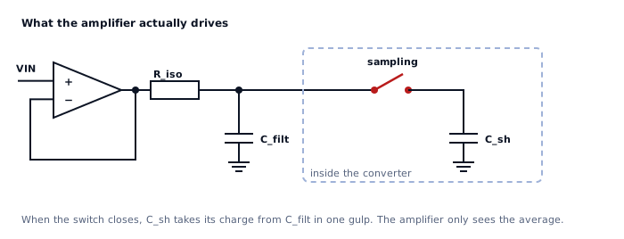
Suppose the sampling capacitor is 20 pF and the input sits at 2.38 V, the full scale of the front end this course carries. At the moment the switch closes, the charge that has to move is:
Q = C_sh · V_in = 20 pF × 2.38 V = 47.6 pCForty-seven picocoulombs is not very much. What makes it awkward is the time it has to move in, which is the acquisition window, a few hundred nanoseconds. A gulp of that size in that time is a current spike of tens of milliamps for a few nanoseconds, and that is what your amplifier is asked to deliver.
This is also the mechanism behind the phrase charge kickback: the same switching event pushes a spike back out into whatever is connected, which is why an unbuffered sensor connected straight to an ADC input can read differently depending on the sample rate.
Where the equivalent resistance comes from
Average the gulps and you get a current:
I_avg = C_sh · V_in · f_sAt 100 kSPS:
I_avg = 47.6 pC × 100 000 = 4.76 µAAnd the equivalent resistance the datasheet quotes is simply the input voltage divided by that:
R_eq = 1 / (f_s · C_sh) = 1 / (100 000 × 20 pF) = 500 kΩNow change nothing but the sample rate:
| Sample rate | Average current | Equivalent resistance |
|---|---|---|
| 10 kSPS | 0.48 µA | 5 MΩ |
| 100 kSPS | 4.76 µA | 500 kΩ |
| 1 MSPS | 47.6 µA | 50 kΩ |
The part did not change. The number did, by two orders of magnitude, because it was never a property of the part on its own.
The error this actually causes
The average current is small, but it has to come through whatever sits between your amplifier and the converter. If that is a series resistor of value R, the current develops a voltage across it:
error = I_avg · RThat voltage is a DC error, present on every reading, and it scales with the input voltage because the charge does. In other words it is a gain error, and it is invisible to an offset calibration.
At 100 kSPS with a 1 kΩ series resistor:
error = 4.76 µA × 1 kΩ = 4.76 mV = 5.9 codesAlmost six codes of gain error, caused by a resistor somebody added as a filter. This is the single most common way a correctly designed signal chain loses accuracy at the last centimetre, and it is the constraint that dominates the next lesson.
Why a bigger capacitor is the obvious answer and not a complete one
The usual fix is a local capacitor at the ADC pin that supplies the gulp, so the amplifier only has to supply the average. Sizing it from the droop:
ΔV = Q / C_filt| C_filt | Droop per sample | In codes |
|---|---|---|
| 1 nF | 47.6 mV | 59 |
| 10 nF | 4.76 mV | 5.9 |
| 100 nF | 0.48 mV | 0.59 |
Reading that table, 100 nF looks obviously right. It is not, and the reason is the subject of lesson 6: the droop does not have to be small, it has to recover before the next sample, and a large capacitor behind a series resistor recovers slowly. The two requirements pull in opposite directions and the design is the compromise between them.
Things this explains
- Readings that change with sample rate. The average current scales with
it, so any series resistance turns the rate into a gain term.
- A multiplexed channel reading high after a high channel. The array keeps
a residue of the previous sample if the acquisition window was short.
- A high-impedance sensor that works on a meter and not on an ADC. A meter
draws nanoamps continuously; an ADC input draws a burst. Source impedance that is fine for one is not for the other.
- A design that worked at 10 kSPS and failed at 500 kSPS with no other
change.
What comes next
Lesson 6 turns all of this into a design: three constraints, a worked choice of resistor and capacitor for a real converter, and which one of the three actually binds.
Sources and further reading
- Microchip: AN246 Driving the Analog Inputs of a SAR A/D Converter — application note, the sampling capacitor, the source resistance and what the two do together.
- Texas Instruments: Sensor to ADC — analog interface design (SLYT173) — journal article, the interface between a source and a converter input treated as one circuit.
- Texas Instruments: A Glossary of Analog-to-Digital Specifications and Performance Measures (SBAA147) — application report, how input impedance and acquisition time are specified.
- Microchip: AN990 Analog Sensor Conditioning Circuits, An Overview — application note, source impedance as a property of the whole chain.