
Why Op Amps Oscillate with Capacitive Loads
One nanofarad is fine and ten is not, and the arithmetic says why to the degree.
- Lesson 9 of 10
- Intermediate
A buffer works on the bench. The same buffer is fitted with a two-metre cable to the sensor head and now the output has a 2 MHz ripple sitting on it that nothing in the schematic can explain.
Nothing is faulty. The cable is a capacitor, the capacitor is inside the feedback loop, and the loop has just been given enough extra phase lag to stop behaving like negative feedback at the frequency where it matters.
Quick answer. An op amp has some output resistance. A capacitive load works against that resistance to form a pole, and because the feedback is taken from the output, that pole sits inside the loop. It adds phase lag exactly where the loop is least able to afford it, which reduces phase margin, which shows up as peaking, overshoot, ringing, or sustained oscillation as the capacitance grows.
Phase margin, defined before it is used
Negative feedback works because the signal coming back is subtracted. Every stage in the loop delays that signal a little, and delay at a given frequency is phase shift. Accumulate enough phase shift and the signal arriving back is no longer being subtracted at that frequency, it is being added, and a loop that adds its own output to its own input is an oscillator.
The frequency that decides this is crossover: the frequency at which the loop gain has fallen to one. Below it the loop has gain to spare. Above it the loop is too weak to sustain anything. At crossover, the question is how much phase shift has already accumulated.
Phase margin is how much phase shift is left before the loop would reinforce rather than oppose. More margin means a better behaved circuit; below roughly 45° you start to see peaking and overshoot; approach zero and the circuit rings for a long time or oscillates outright.
An internally compensated op amp is designed to contribute most of a right-angle of phase shift at crossover all by itself, leaving a healthy margin for the circuit around it. Spending that margin is what a capacitive load does.
The arithmetic, with real numbers
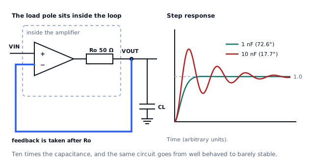
The amplifier's output is not a perfect voltage source. There is some resistance between the internal node and the pin. Take 50 Ω, which is unremarkable for a general-purpose part, and suppose the loop crosses over at 1 MHz, as a 1 MHz amplifier does when used as a unity-gain buffer.
A capacitance CL on the output forms a pole with that resistance at:
f = 1 / (2π · Ro · CL)With CL = 1 nF:
f = 1 / (2π × 50 × 1×10⁻⁹) = 3.18 MHzThe pole is well above crossover. The phase lag it contributes at 1 MHz is:
arctan(1 MHz / 3.18 MHz) = 17.4°Starting from the amplifier's own 90°, the phase margin is about 180 − 90 − 17.4 = 72.6°. Comfortable.
With CL = 10 nF:
f = 1 / (2π × 50 × 10×10⁻⁹) = 318 kHz
arctan(1 MHz / 318 kHz) = 72.3°
Phase margin is now about 180 − 90 − 72.3 = 17.7°. That is a circuit that rings heavily on a step and peaks several decibels in frequency response, and a modest amount of extra lag from anywhere else would finish the job.
Ten times the capacitance, and a circuit went from well behaved to barely stable. That ratio, not the exact degrees, is what to take away.
Be clear about what the arithmetic is for. The assumption that the amplifier contributes exactly 90° is an idealisation of a single-pole model, real parts have additional poles that make the true margin lower, and output resistance is itself frequency dependent rather than a fixed 50 Ω. The calculation explains the mechanism and predicts the scaling. It does not replace the datasheet's own curves of overshoot against load capacitance, which are measured rather than assumed.
Where the capacitance comes from
It is rarely a component someone chose. The usual sources, roughly in order of how often they surprise people:
- Cable. Coaxial and ribbon cable runs tens to over a hundred picofarads
per metre. A short cable is a real load.
- The next stage's input. The sampling capacitor at an ADC input is a
capacitive load, and it is switched, which makes it worse.
- A filter capacitor placed at the output. Putting the filter after the
amplifier instead of before it is a very common way to create this problem.
- A long PCB trace to a distant connector, particularly over a plane.
- A scope probe, which is why a circuit can be stable until you measure
it, and occasionally the reverse.
What to do about it, and what each remedy costs
There is no universal resistor value, and anyone offering one is guessing on your behalf. Here is what the available approaches actually trade.
A series isolation resistor. Put a resistor between the amplifier output and the capacitance, and take the feedback from the amplifier side. The load pole is now outside the loop and the loop is stable again.
The cost is immediate and often disqualifying. That resistor carries the load current, so with 50 Ω and 10 mA of load:
error = 50 Ω × 10 mA = 500 mVHalf a volt of DC error at the load, which the feedback cannot correct because the feedback is not measuring the load. For a high-impedance destination, such as an ADC input that draws almost nothing, this is close to free and is usually the right answer. For anything that draws current it is not.
Isolation resistor with feedback from the load. Take the DC feedback from the far side of the resistor so the loop corrects the drop, and add a small capacitor providing high-frequency feedback from the amplifier side. DC accuracy is restored, and the price is bandwidth and a compensation network that has to be designed rather than copied.
A snubber. A resistor and capacitor in series from the output to the reference node, sized to damp the resonance. It does not introduce a DC error, because no DC flows through a capacitor. It does load the output at high frequencies and dissipate a little power.
Raise the noise gain. A loop crossing over at a higher gain crosses over at a lower frequency, where the load pole has contributed less lag. This is why a buffer at unity gain is the hardest case and the same amplifier at a gain of ten may be untroubled. Recall from lesson 2 that it is noise gain that counts, so this can be done with components that do not change the signal gain, at the cost of amplifying input errors and noise more.
Choose a part designed for it. Some amplifiers specify a capacitive load they will drive directly, with overshoot curves to prove it. If the load is known and fixed, this is the cheapest fix available, because it costs a part number rather than components and accuracy.
Before blaming the load
| Symptom | Likely cause | What to check first |
|---|---|---|
| Ringing that worsens as CL rises | load pole inside the loop | the load capacitance, including cable |
| Oscillation at a fixed frequency regardless of load | supply decoupling or layout | decoupling at the supply pins |
| Peaking in the frequency response, no visible ringing | reduced but not lost phase margin | noise gain, load, stray capacitance |
| Instability only in unity-gain buffer | worst case for phase margin | whether the part is unity-gain stable |
| Ringing that appears when the probe is attached | the probe is the load | measure with a lower-capacitance probe |
That second row deserves emphasis. An amplifier whose supply pins are not properly decoupled can oscillate on its own, and it will look exactly like a load problem while being nothing of the kind. Checking the decoupling before redesigning the output network takes a minute and sometimes ends the investigation, which is why capacitor placement is worth reading in the power integrity course.
Capacitance at the inverting input does the same thing by a different route, forming a pole with the feedback network rather than with the output resistance. Stray capacitance at that node is easy to acquire from a long trace or a socket, and the fix is usually a small capacitor across the feedback resistor rather than anything at the output.
The same idea, elsewhere
Phase margin is not an op-amp concept. It is a property of any feedback loop, and the same reasoning explains why a switching regulator rings or oscillates when its output capacitance is changed, which is worked through in the regulator stability lesson of the switching course. Recognising it as one phenomenon rather than two is most of the value.
What comes next
Lesson 10 collects every limit in this course into a way of choosing a part: not a recommendation, but an order in which to apply the constraints so that the shortlist shrinks for reasons you can defend.
Sources and further reading
- Texas Instruments: Op amp stability and input capacitance (SLYT087) — journal article, loop gain as the thing that determines stability, and capacitance at the inverting input as a cause.
- Texas Instruments: AN-1708 LMV841 Stability Considerations (SNOA502) — application note, capacitive load behaviour and reducing overshoot on a specific device.
- Texas Instruments: Feedback Plots Define Op Amp AC Performance (SBOA015) — application bulletin, reading stability off the gain and phase curves.
- Microchip: AN723 Operational Amplifier AC Specifications and Applications — application note, the AC specifications involved and their circuit consequences.