
Common-Mode Input Range: Why an Op Amp Can Fail Before It Saturates
The output is nowhere near a rail, the arithmetic is right, and the reading is still wrong.
- Lesson 7 of 10
- Intermediate
There is a comfortable assumption behind a lot of analog debugging: if the output is not stuck at a supply rail, the amplifier must be working. The output is at 3.3 V on a 5 V supply, which is a long way from both rails, so whatever is wrong must be somewhere else.
It is not a safe assumption. An op amp has a second range, separate from the output range, and when the inputs leave it the amplifier can produce an output that is entirely plausible and entirely wrong.
Quick answer. Input common-mode range is the window of voltage within which the input pins themselves must stay for the amplifier to behave as specified. It is set by the transistors in the input stage and their headroom to the supply rails, and it is a different limit from how close the output can get to a rail. Exceed it and the amplifier does not necessarily saturate. It can carry on producing an output near where you expected, with a much larger error than the datasheet promises.
Common mode and difference are two separate things
Every pair of input voltages can be described two ways. The differential voltage is the difference between them, which is what the amplifier is meant to amplify. The common-mode voltage is roughly their average, which is where the pair is sitting.
An ideal amplifier would ignore the common-mode voltage entirely. A real one mostly does, over a limited range, and does something else outside it.
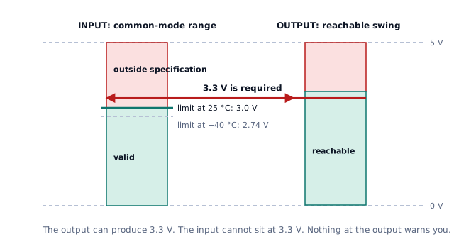
The reason is in the figure. The input stage is a differential pair of transistors with a current source above or below it. Each of those devices needs some voltage across it to stay in its useful operating region. Add them up and you get a band of common-mode voltage within which the stage behaves like an amplifier, and some distance to one or both rails where it does not.
Which rail you lose depends on the input stage. A PNP or PMOS pair works comfortably down to the negative rail, and sometimes slightly below it, while running out of room some way short of the positive rail. An NPN or NMOS pair is the mirror image. A part that claims to handle the whole span usually has both, which brings a problem of its own, covered in the next lesson.
What the datasheet actually says
Take a device from the widely used general-purpose family typified by the LM324 and LM358. Its recommended input common-mode range is from the negative supply up to VCC − 2 V over the full temperature range. On a 5 V supply that is 0 V to 3.0 V, not 0 V to 5 V.
Two details in that sentence do a lot of work.
The limit is expressed relative to a rail, not as an absolute voltage. Run the same part from 3.3 V and the window becomes 0 V to 1.3 V, which is less than half the supply. People who verified a design at 5 V and then dropped the rail to save power have been caught by exactly this.
And the limit moves with temperature. For this family the upper limit varies by roughly 4 mV/°C, and cold reduces it. Going from 25 °C down to −40 °C is 65 °C:
shift = 4 mV/°C × 65 °C = 260 mVSo the upper limit falls from 3.0 V to about 2.74 V. A circuit whose common-mode voltage is 2.9 V has 100 mV of margin on the bench at room temperature and is 160 mV outside the specification in a cold chamber. That is a textbook example of a design that passes final test and fails in the field, and it is also why the specification is written over the full temperature range rather than at 25 °C.
The example where everything looks fine
Here is the case that produces the most wasted afternoons.
You need a buffered 3.3 V reference on a board whose analog supply is 5 V. You put a voltage reference into a unity-gain follower built from one half of a general-purpose dual op amp, and you measure the output.
- Expected output: 3.3 V.
- Output range of this part on a 5 V supply with a light load: it can reach
above 3.3 V, so the output is not saturated.
- Input common-mode voltage: also 3.3 V, because in a follower the input pin
sits at the signal.
- Specified limit at 25 °C: 3.0 V.
The circuit is operating 300 mV outside its input common-mode range while its output sits comfortably mid-scale. At −40 °C that margin violation grows to 560 mV.
What you measure is a voltage somewhere near 3.3 V. Not a rail, not zero, not obviously broken. The error is whatever the input stage does once it is out of its region: a much larger effective offset, a gain that is no longer what you derived, and a temperature coefficient nothing in the datasheet describes, because the datasheet does not describe operation there at all.
The failure is that the part is being used outside its specification, so there is no number you can look up to predict the result. Two samples from the same reel may differ. The same sample may behave differently next week.
Below the negative rail, it gets worse
Exceeding the upper limit degrades accuracy. Going below the negative rail can do something more dramatic.
If an input is taken more than a few hundred millivolts below the negative supply, parasitic junctions inside the input structure begin to conduct. For this family the threshold quoted is around −0.3 V with respect to the negative supply. Significant current then flows into the input pin, and the output can reverse: a condition called phase reversal or output phase inversion, in which the output slams to the wrong rail entirely.
In a feedback loop that is a genuine fault, because the loop that was keeping everything in order has just had its sign changed.
The part that catches people is where the negative excursion comes from. It is rarely the signal. It is ground bounce, switching noise coupled from a nearby converter, or an inductive source ringing below zero for a few hundred nanoseconds. A board whose analog reference is not actually at the same potential as the amplifier's negative supply pin is a board that can produce this on its own, which makes it a layout question as much as a circuit one. How a shared return develops those millivolts is the subject of the mixed-signal grounding lesson in the grounding course.
One exception worth knowing
When one of these parts is used as a comparator rather than an amplifier, only one input has to be inside the common-mode range for the output to go the expected way. The other may sit above the range, and the output still resolves correctly. If both inputs are above the range, the output is undefined and may differ from part to part.
This is a real and documented allowance, and it is also a trap, because it applies to open-loop comparison and not to the amplifier circuits this course is about. It is worth knowing mostly so you do not generalise it in the wrong direction.
Checking it in a design review
| Question | Why it matters |
|---|---|
| What is the common-mode voltage at every input, over the whole signal range? | This is the quantity the limit applies to, and it is not always obvious |
| Is the limit specified relative to a rail? | Then changing the supply changes the limit |
| Is the specification over temperature or at 25 °C? | Cold moves this limit on many bipolar parts |
| Can any input go below the negative supply, even briefly? | Phase reversal and input current, not just error |
| Is the negative supply pin at the same potential as the signal's reference? | If not, the amplifier sees a different common-mode voltage than you drew |
| Is the output near mid-scale? | Then nothing about the output will warn you |
That last row is the point of the lesson. Output saturation is a visible symptom. A common-mode violation is not.
What comes next
Lesson 8 takes the obvious response to all of this, which is to reach for a part advertised as rail-to-rail, and examines what that phrase does and does not promise.
Sources and further reading
- Texas Instruments: Application Design Guidelines for LM324 and LM358 Devices (SLOA277B) — application note, the common-mode range of this family, its temperature coefficient, the comparator allowance and the conditions that cause phase reversal.
- Texas Instruments: Understanding Operational Amplifier Specifications (SLOA011) — application report, common-mode range among the input specifications and how it is tested.
- Microchip: AN682 Using Single Supply Operational Amplifiers in Embedded Systems — application note, why input range becomes a binding constraint when there is no negative rail.
- Texas Instruments: Trade-offs Between CMOS, JFET, and Bipolar Input Stage Technology (SBOA355) — application report, how the input stage technology sets the common-mode range.