
How a Buck Converter Actually Works
Two switch states, one inductor, and where the current goes in each.
- Lesson 1 of 10
- Intermediate
A linear regulator makes 3.3 V from 12 V by turning the other 8.7 V into heat. At 2 A that is 17.4 W of heating, which is why nobody does it.
A buck converter makes the same rail by connecting the output to 12 V for part of the time and to 0 V for the rest, then averaging the result with an inductor and a capacitor. Nothing dissipates the difference because nothing has to: the energy is stored and released rather than burned.
Everything else in this course follows from understanding those two states properly.
Quick answer. A buck converter switches its input on and off, and filters the resulting square wave with an inductor and capacitor. While the switch is closed, current flows from the input through the inductor to the load and the inductor stores energy. When the switch opens, the inductor keeps that current flowing through a second switch or a diode to ground. The output settles near the input voltage multiplied by the fraction of time the switch is closed.
The two states
Three components carry the current: a high-side switch from the input, a low-side switch or diode to ground, and an inductor from their junction to the output. That junction is the switch node, and lesson 9 is entirely about it.
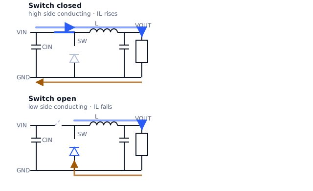
Switch closed. The inductor sees the input voltage on one end and the output voltage on the other. The voltage across it is VIN − VOUT, which is positive, so the current through it rises. That current goes to the load and to the output capacitor. Current also flows from the input capacitor, which matters enormously and is lesson 6.
Switch open. The inductor current cannot stop instantly, because stopping it would require infinite voltage. It keeps flowing in the same direction, and the low-side device provides the path back from ground. Now the inductor has the output voltage across it with the opposite sign, so the current falls.
Two things to notice, because they are the source of most confusion later:
- The inductor current never reverses in normal operation. It ramps up, then
ramps down, around an average equal to the load current.
- The input current is chopped. It flows only while the high-side switch
is closed. The output current is continuous. That asymmetry is the whole reason the input capacitor has a harder job than the output capacitor.
Where the duty cycle comes from
In steady state the inductor current ends each cycle where it started. Otherwise it would grow without limit. That single constraint gives you the transfer function without any further theory.
The current rise during the on-time has to equal the fall during the off-time:
(VIN − VOUT) · t_on = VOUT · t_off
Divide through by the period and rearrange, and with D = t_on / T:
VOUT = VIN · D
For a 12 V input and a 3.3 V output:
D = VOUT / VIN = 3.3 / 12 = 0.275
So the switch is closed about 27.5 % of each cycle. At a switching frequency of 500 kHz the period is 2 µs, so the on-time is roughly 550 ns.
This is the ideal relationship. A real converter needs a slightly longer on-time, because the switches have resistance and the inductor has some of its own, and those drops have to be made up. For a first estimate the ideal expression is close enough to be useful, and knowing that the real duty cycle runs a little higher is usually all the correction you need.
What the inductor is for
A common description is that the inductor "smooths" the output. True, but it obscures what is actually happening, which is energy transfer.
An inductor resists changes in current. Put a voltage across it and the current ramps rather than jumps, at a rate di/dt = V / L. During the on-time the converter is pushing energy into the inductor's magnetic field. During the off-time it takes that energy back out and delivers it to the output.
The capacitor is the other half. Inductor current is a triangle wave, while the load wants a steady current. The capacitor absorbs the difference, charging slightly when the inductor delivers more than the load needs and discharging when it delivers less. That small charge and discharge is the output ripple voltage, which lesson 7 computes.
Continuous and discontinuous
At reasonable load, the inductor current stays above zero for the whole cycle. The current is a triangle sitting on a DC level. This is continuous conduction mode, and it is the case all the arithmetic above assumes.
Reduce the load far enough and the average current gets smaller than half the ripple. The current would have to go negative during part of the cycle to keep the triangle centred. With a diode as the low-side device it cannot, because a diode conducts one way. The current hits zero and stays there until the next cycle begins. This is discontinuous conduction mode.
Two practical consequences:
- In discontinuous mode
VOUT = VIN · Dno longer holds. The duty cycle
needed for a given output now depends on the load, and the controller adjusts it for you.
- A converter with a synchronous rectifier, meaning a transistor rather than
a diode on the low side, can let the current reverse. Many such parts offer both behaviours, switching to a mode that skips pulses at light load to avoid wasting energy pushing current backwards.
You do not need to design for discontinuous mode on a typical board. You do need to recognise it, because a converter that looks fine at full load and behaves oddly at 50 mA has usually crossed into it.
What this already tells you
Before any component is chosen, the two states have told you where the difficult currents are.
- The loop carrying chopped current is input capacitor, high-side switch,
low-side device, and back. That loop sees the full switching edge. Keeping it tiny is lesson 6.
- The switch node swings between roughly the input voltage and roughly
ground, at whatever edge rate the device manages. It is the aggressor in every coupling problem on the board, which is lesson 9.
- The inductor carries the load current plus a triangular ripple on top, and
both parts of that matter when selecting it, which is lesson 5.
What comes next
Lesson 2 runs the same analysis on a boost converter, where the output is higher than the input and the uncomfortable consequence is what happens to the input current.
Sources and further reading
- Analog Devices: Buck Power Stage Design Equations — application note, steady-state relationships for the buck power stage.
- Texas Instruments: LM60430 / LM60440 datasheet — datasheet, buck operating description and the input loop it identifies as most critical.
- Analog Devices: Selecting the Right Inductor Current Ripple — technical article, inductor current behaviour across conduction modes.
- onsemi: LC Selection Guide for the DC-DC Synchronous Buck Converter (AND9135) — application note, synchronous buck operation and the role of each switch.