
Input Offset Voltage: How Small Errors Become Large Output Errors
150 microvolts at the input is 22 converter codes at the output, and calibration only removes part of it.
- Lesson 5 of 10
- Intermediate
Our front end amplifies 20 mV by 119 and hands 2.38 V to a 12-bit converter. One converter code is worth 6.8 µV at the input. An amplifier whose datasheet promises a maximum offset of 150 µV therefore starts 22 codes wrong before the sensor has done anything.
That is the whole problem with input offset voltage. It is a small number that arrives at the input, and it leaves through the same multiplier as the signal.
Quick answer. Input offset voltage is a small DC error, typically tens to hundreds of microvolts, that behaves as though it were added in series with one of the inputs. The output sees it multiplied by the circuit's noise gain, not by its signal gain. It can be calibrated out at one temperature, but its drift with temperature cannot, which is why the drift specification often matters more than the offset specification.
Where it comes from and why it has a sign
An op amp's input stage is a matched pair of transistors. Matched is a manufacturing goal, not a physical law, and the residual mismatch means the output is not exactly zero when the inputs are at exactly the same voltage.
Input offset voltage is the differential input you would have to apply to bring the output back to zero. Treating it as a small battery in series with one input is a good working model, because it behaves like one in every calculation.
Two properties of that battery matter and are frequently forgotten. Its polarity is not known: the datasheet gives a magnitude, and the actual sign differs from part to part. And its value is not fixed: it moves with temperature, with supply voltage and with common-mode voltage, each of which has its own specification.
The arithmetic on our front end
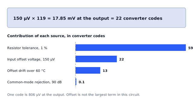
Assumptions: non-inverting stage, Rf = 118 kΩ, Rg = 1 kΩ, noise gain 119, full scale 2.38 V, 12-bit converter on a 3.3 V reference so one code is 806 µV. The amplifier is specified at VOS maximum 150 µV at 25 °C with a drift of 1.5 µV/°C.
The output error is the offset times the noise gain:
VOUT(error) = VOS × noise gain = 150 µV × 119 = 17.85 mVExpress that three ways, because each one persuades a different audience:
- 17.85 mV at the output.
- 0.75 % of the 2.38 V full-scale reading.
- 22 codes of the converter, from 17.85 mV / 806 µV.
Note which gain did the multiplying. If you had built the inverting version from lesson 2, with a signal gain of 118, the output offset would still be 17.85 mV, because noise gain is 119 in both circuits. The error does not care about the sign of your signal.
Drift is the part calibration cannot reach
A single-point calibration at room temperature measures the output with the sensor at zero and subtracts whatever it finds. That removes the 150 µV, and it removes it well. It does not remove what happens next.
Take an operating range up to 85 °C, calibrated at 25 °C. The temperature excursion is 60 °C, and at 1.5 µV/°C:
ΔVOS = 1.5 × 60 = 90 µV
output error = 90 µV × 119 = 10.71 mV ≈ 13 codes
Thirteen codes of error that no amount of calibration at 25 °C will touch, because it was not there when you calibrated. This is the usual reason a product passes final test and fails in the field, and it is why the drift figure deserves at least as much attention as the headline offset.
Two further points on drift, both of which cost people time:
- Drift is not necessarily linear and not necessarily one-signed. The
specification is normally an average over the range, not a slope you can trust at every point.
- Trimmed parts are not automatically low-drift parts. Factory trimming
reduces the initial offset at one temperature. Some trim techniques improve drift and some do not, and the two parameters have separate specifications for a reason.
Offset is not the only DC error, and here it is not the largest
It would be convenient if offset were the dominant term. In this circuit it is not, and a lesson that implied otherwise would be teaching a bad habit.
Our gain of 119 is made from two resistors. At 1 % tolerance, the worst combination of Rf high and Rg low gives:
G = 1 + (118 kΩ × 1.01) / (1 kΩ × 0.99) = 121.4That is 2.0 % above nominal, which at full scale is 47.7 mV, nearly three times the offset error. Worst-case stacking is pessimistic, and a root-sum- square estimate of two independent 1 % parts gives about 1.4 %, but either figure dominates the offset term.
| Error source | Contribution at full scale | Removed by one-point calibration? |
|---|---|---|
| Resistor tolerance, 1 % | about 48 mV worst case | no, it is a gain error |
| Offset voltage, 150 µV | 17.85 mV | yes, at the calibration temperature |
| Offset drift, 60 °C excursion | 10.71 mV | no |
| Bias current into source resistance | depends on the source, see lesson 6 | partly |
| Common-mode rejection, 90 dB | about 0.08 mV here | no, it tracks the signal |
| Amplifier and resistor noise | not a DC term, but sets the floor | no |
The common-mode entry is worth a sentence because it is so often quoted out of context. In this non-inverting stage the input common-mode voltage is the sensor signal itself, so it moves only 20 mV over the full range. With a common-mode rejection ratio of 90 dB that produces an input-referred error of about 0.63 µV, which is a tenth of a converter code. The same specification in a difference amplifier with several volts of common mode would produce an error hundreds of times larger. The parameter has not changed; the circuit has.
The practical conclusion is an ordering, not a ranking of parts. Fix the gain error first, with tighter resistors or a two-point calibration that measures gain as well as offset. Then offset drift. Then initial offset, which is the one your calibration already handles.
Ground is part of this budget too. The amplifier measures its input against whatever its reference node is actually at, and a millivolt of drop in a shared return path is indistinguishable from a millivolt of offset. Where that drop comes from is the subject of the return current lesson in the grounding course.
What comes next
Lesson 6 takes the one row of the table we left open, the current the inputs draw, and shows why it can be irrelevant in one circuit and the dominant error in the next one, with the same amplifier.
Sources and further reading
- Microchip: AN1747 Operational Amplifier Applications Using 8-Bit PIC Microcontrollers — application note, offset and bias current as entries in a DC error budget.
- Microchip: AN722 Operational Amplifier Topologies and DC Specifications — application note, the DC specifications and how a gain stage multiplies them.
- Texas Instruments: Understanding Operational Amplifier Specifications (SLOA011) — application report, offset, drift and the conditions under which they are specified.
- Texas Instruments: Feedback Plots Define Op Amp AC Performance (SBOA015) — application bulletin, noise gain as the multiplier for input-referred errors.