
Inverting vs Non-Inverting Op Amps: What Actually Changes
Same two resistors, two circuits, and three differences the gain equations never show.
- Lesson 2 of 10
- Intermediate
The two basic op-amp stages are usually taught as a pair of equations, which makes them look like alternatives you pick by whether you want a minus sign. That is not what separates them in practice.
This lesson builds both with the same two resistors, so the only thing that changes is the topology, and then looks at what actually differs. The answer is three things, and signal polarity is the least important of them.
Quick answer. A non-inverting stage has a gain of 1 + Rf/Rg and an input impedance set by the op amp, which is very high. An inverting stage has a gain of −Rf/Rg and an input impedance equal to Rg, which is whatever you made it. Both have the same noise gain, 1 + Rf/Rg, so both suffer the same offset error and both get the same bandwidth from the same amplifier. The choice is usually decided by what is driving the input, not by the sign.
The circuit this course keeps coming back to
A sensor produces 0 to 20 mV. It is read by a 12-bit converter on a single 3.3 V supply, and we want to use most of the converter's range without running into either rail, so we aim for about 2.4 V at full scale.
The gain required is 2.4 / 0.020 = 120. With standard 1 % values, Rg = 1.00 kΩ and Rf = 118 kΩ give:
G = 1 + Rf/Rg = 1 + 118 000 / 1 000 = 119Full-scale output is 119 × 20 mV = 2.38 V. Close enough to the target, and built from two parts you can actually buy.
One converter code is worth 3.3 / 4096 = 806 µV at the output, which referred back to the input is 806 µV / 119 = 6.8 µV. Remember that number. It is the yardstick every error in this course gets measured against.
The same resistors, the other way round
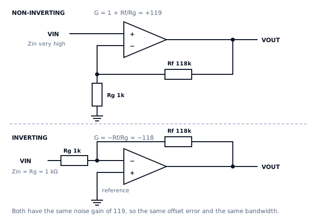
Keep Rf = 118 kΩ and Rg = 1 kΩ and rebuild the stage as an inverting amplifier. Now the signal drives Rg, the free end of Rg is the input, and the non-inverting pin goes to a reference.
G = −Rf/Rg = −118 000 / 1 000 = −118Not −119. The inverting and non-inverting gains from an identical resistor pair differ by exactly one, which matters less than the fact that people routinely assume they are the same magnitude.
Difference one: what the source sees
In the non-inverting stage the signal arrives at the amplifier's own input pin. That pin draws a bias current, which we will deal with in a later lesson, but it does not present a resistance to ground. The source is barely loaded.
In the inverting stage the signal drives Rg into a node held at a fixed voltage by the feedback. The input impedance is therefore Rg, and nothing else. Here that is 1 kΩ.
Now suppose the sensor has 10 kΩ of its own source resistance. The inverting stage does not see a 20 mV source any more, it sees 20 mV behind 10 kΩ feeding 11 kΩ in total:
G = −Rf / (Rs + Rg) = −118 000 / 11 000 = −10.7The gain has collapsed from 118 to 10.7, an error of about 91 %. The non-inverting stage with the same sensor is essentially unaffected.
This is the single most common reason to choose between the two, and it has nothing to do with polarity.
Difference two: noise gain is the same, signal gain is not
Offset voltage, input noise and anything else that appears as an error at the amplifier's input gets multiplied by the noise gain, which is the gain from the inverting input to the output:
noise gain = 1 + Rf/Rg = 119For the non-inverting stage that happens to equal the signal gain. For the inverting stage it does not: signal gain 118, noise gain 119. The inverting amplifier amplifies its own errors slightly more than it amplifies your signal, and at low gains the discrepancy becomes dramatic. An inverting stage with Rf = Rg has a signal gain of 1 and a noise gain of 2, and an inverting attenuator with a signal gain of −0.5 still has a noise gain of 1.5.
Two consequences follow, and both are easy to miss:
- The offset error is the same in both circuits. It is noise gain that
multiplies offset, so both of our stages turn an input offset into 119 times as much output offset, even though one has a signal gain of 118.
- The bandwidth is the same in both circuits. It is also noise gain that
divides the gain-bandwidth product, which the next lesson works through. Building the inverting version does not buy you speed.
Difference three: where the reference node is
In the non-inverting stage the output is referred to whatever the non-inverting pin is tied to. In the inverting stage, the inverting node is held at whatever the non-inverting pin is tied to, and the output swings around that same voltage.
On a split supply both are usually ground and nobody thinks about it. On a single supply, which is what our front end uses, it becomes a design decision with real consequences.
Our sensor's output is referenced to ground and sits near 0 V. For the non-inverting stage that means the amplifier's input common-mode voltage is also near 0 V, and the output must be able to approach 0 V as well, because the bottom of the sensor range maps to the bottom of the output range. Both of those are requirements on the part, not on the resistors, and both are covered later in this course.
The inverting version is worse here, not better. Its input node would have to sit at the non-inverting pin's voltage, and a 0 to 20 mV positive input would drive the output negative, which a single supply cannot provide. Making it work needs a reference somewhere above ground and a different mapping of the range, which is extra parts and extra error sources.
Choosing between them
| Question | Favours non-inverting | Favours inverting |
|---|---|---|
| Source impedance is high or unknown | yes | no |
| The source cannot tolerate loading | yes | no |
| You need to sum several signals | no | yes, at the virtual node |
| You need gain below 1 | no | yes |
| You need the signal inverted | no | yes |
| Single supply, signal referenced to ground | usually | needs a reference |
| Input common-mode range is tight | no | yes, the input pin sits still |
That last row deserves a note, because it is the one argument for the inverting stage that has nothing to do with polarity or impedance. In an inverting amplifier the non-inverting pin is tied to a fixed voltage and the inverting node is held there by the loop, so the input common-mode voltage never moves regardless of how large the signal is. In a non-inverting amplifier the common-mode voltage is the signal. When common-mode range is the binding constraint, that is decisive.
What comes next
Lesson 3 takes the noise gain of 119 established here and shows what it does to the bandwidth of the stage, which is a larger effect than most people expect from a part advertised at 1 MHz.
Sources and further reading
- Texas Instruments: AN-20 An Applications Guide for Op Amps (SNOA621) — application report, the configurations and the error terms each one carries.
- Texas Instruments: Feedback Plots Define Op Amp AC Performance (SBOA015) — application bulletin, noise gain as the quantity that governs both error and bandwidth.
- Microchip: AN722 Operational Amplifier Topologies and DC Specifications — application note, the DC consequences of each topology.
- Microchip: AN682 Using Single Supply Operational Amplifiers in Embedded Systems — application note, what changes when there is no negative rail to refer to.